Self-correcting crystal may lead to the next generation of advanced communications
November 7, 2013
[+]
A five-year, multidisciplinary collaborative research effort based at
Cornell has resulted in the world’s best material for tunable
capacitors — broadly called a tunable dielectric, a special insulator
whose ability to store electrical charge changes when a voltage is
applied.
High
magnification image of the new tunable dielectric material, taken with
Cornell’s scanning transmission electron microscope. The atomic
structure resembles a brick wall in which the horizontal and vertical
lines, the “mortar,” are believed key to the performance of the
material. (Credit: Ye Zhu/Muller group)
“This is a radically different material compared to what people have been using for decades,” said Darrell Schlom, the Herbert Fisk Johnson Professor of Industrial Chemistry at Cornell, who led the international team.
“What we have discovered is the world’s lowest-loss tunable dielectric.” (“Loss” refers to wasted energy, which drains cell phone batteries.)
The Cornell-designed-and-created new type of tunable dielectric could greatly improve the performance of microwave circuit capacitors found in every cell phone and open up new possibilities for wireless communication at much higher frequencies.
The scientific achievement is twofold. It is the material itself, a layered strontium titanium oxide – not found in nature – created through molecular beam epitaxy, which Schlom’s lab uses to build up layered materials one atomic layer at a time by “spraying” atoms onto a surface.
The other breakthrough is the “materials by design” method used to make the material have the desired properties.
The tunable dielectric and its properties were first envisioned on paper, tested on the computer, created in the lab atom by atom, patterned into a capacitor device and, finally, verified with electrical measurements. The result is a tunable dielectric capacitor with at least five times the performance of commercial tunable capacitors available today, according to Schlom.
By comparison, today’s commercially used tunable dielectric material is not a layered material and contains barium in addition to strontium, oxygen and proprietary additives. Thin films of such materials are rife with defects, which waste power and greatly lower the films’ performance in circuits — a problem cell phone companies would like to solve.
A ‘forgiving’ thin film
The Cornell thin film could be the answer. An atomic-resolution electron micrograph reveals its design. It looks like bricks and mortar, with very specific spacing between the well-defined interfaces. The layered structure is “forgiving” with regard to defects, Schlom said: The “mortar” portions seem to soak up many of the defects, which keep them away from the “bricks,” drastically improving the performance of this new variety of tunable capacitors.
The proof-of-principle demonstration of the new strontium titanium oxide requires further testing to confirm how the defects in the material are being mitigated and how to push its performance even further.
“It is clear that we have discovered a killer material,” Schlom said, “but it is likely that even better tunable dielectrics can be found using our approach.”
Tunable dielectrics also work well in the microwave range and beyond — modern communications applications like cell phones typically use frequencies around a few gigahertz
“These new materials work well up to 100 GHz, opening the door for the next generation of devices for advanced communication,” says National Institute of Standards and Technology (NIST) materials scientist Nathan Orloff. Higher-frequency devices can handle higher data communication speeds.
[+]
Self-correcting crystals
Applying strain within the strontium titanate crystal structure to test for tunability (credit: Che-Hui Lee et al./Nature)
Modern cellphone dielectrics use materials that suffer from misplaced or missing atoms called “defects” within their crystal structure, which interfere with the dielectric properties and lead to power loss.
One major feature of the new materials, says Orloff, is that they self-correct, reducing the effect of defects in the part of the crystal where it counts.
“We refer to this material as having ‘perfect faults’,” he says. “When it’s being grown, one portion accommodates defects without affecting the good parts of the crystal. It’s able to correct itself and create perfect dielectric bricks that result in the rare combination of high tuning and low loss.”
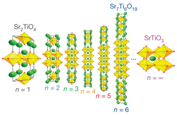
The new material has layers of strontium oxide, believed to be responsible for the self-correcting feature, separating a variable number of layers of strontium titanate.
The sandwich layers are grown as a thin crystalline film on top of a substrate material with a mismatched crystal spacing that produces strain within the strontium titanate structure that makes it a less stable dielectric — but one that can be tuned.
The work was supported by the Army Research Office and the National Science Foundation, including the Cornell Center for Materials Research and the NSF Materials Research Science and Engineering Centers program.
Abstract of Nature paper
The miniaturization and integration of frequency-agile microwave circuits — relevant to electronically tunable filters, antennas, resonators and phase shifters — with microelectronics offers tantalizing device possibilities, yet requires thin films whose dielectric constant at gigahertz frequencies can be tuned by applying a quasi-static electric field1. Appropriate systems such as BaxSr1−xTiO3 have a paraelectric–ferroelectric transition just below ambient temperature, providing high tunability. Unfortunately, such films suffer significant losses arising from defects. Recognizing that progress is stymied by dielectric loss, we start with a system with exceptionally low loss — Srn+1TinO3n+1phases — in which (SrO)2 crystallographic shear planes provide an alternative to the formation of point defects for accommodating non-stoichiometry. Here we report the experimental realization of a highly tunable ground state arising from the emergence of a local ferroelectric instability in biaxially strained Srn+1TinO3n+1 phases with n ≥ 3 at frequencies up to 125 GHz. In contrast to traditional methods of modifying ferroelectrics — doping or strain — in this unique system an increase in the separation between the (SrO)2 planes, which can be achieved by changing n, bolsters the local ferroelectric instability. This new control parameter, n, can be exploited to achieve a figure of merit at room temperature that rivals all known tunable microwave dielectrics.
(¯`*• Global Source and/or more resources at http://goo.gl/zvSV7 │ www.Future-Observatory.blogspot.com and on LinkeIn Group's "Becoming Aware of the Futures" at http://goo.gl/8qKBbK │ @SciCzar │ Point of Contact: www.linkedin.com/in/AndresAgostini
 Washington