QUANTA

Wednesday, November 27, 2013

Sony files patent for wearable-electronics wig

November 27, 2013
[+]
(Credit: USPTO)
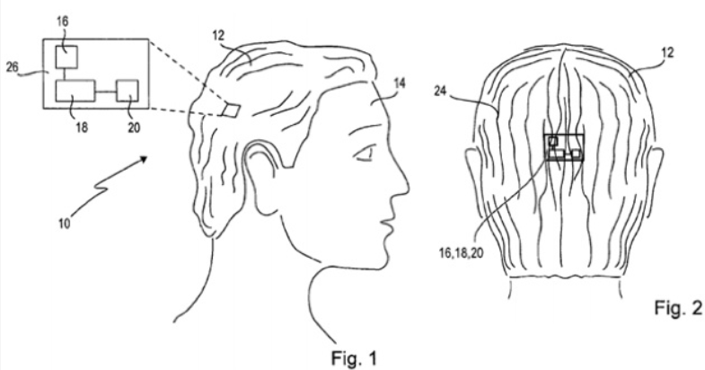
Sony has filed a patent for a wig with wearable electronic devices that could be “visually hidden” and controlled.
“The usage of a wig has several advantages that, compared to known wearable computing devices, include significantly increased user comfort and an improved handling of the wearable computing device,” Sony said in its patent application.
Sony claims include a variety of wearable devices that could be embedded (and hidden) in the hair, such as a camera, laser pointer, computer, or electronics to control wearable devices such as “computer glasses” or smart phones.
Other uses mentioned: help blind people navigate (using GPS and tactile stimulator devices), gaming, and virtual reality devices.
Comb-over cloaking was not mentioned in the patent application.


(¯`*• Global Source and/or more resources at http://goo.gl/zvSV7 │ www.Future-Observatory.blogspot.com and on LinkeIn Group's "Becoming Aware of the Futures" at http://goo.gl/8qKBbK │ @SciCzar │ Point of Contact: www.linkedin.com/in/AndresAgostini

Talk to Google on Chrome

November 27, 2013
Now you can talk to Google whenever you’re using Chrome — hands-free, no typing. Simply say “Ok Google” and then ask your question.
To access hands-free search on your laptop, just download the free Google Voice Search Hotword extension from the Chrome Web Store (available in English in the U.S.).


(¯`*• Global Source and/or more resources at http://goo.gl/zvSV7 │ www.Future-Observatory.blogspot.com and on LinkeIn Group's "Becoming Aware of the Futures" at http://goo.gl/8qKBbK │ @SciCzar │ Point of Contact: www.linkedin.com/in/AndresAgostini

Creating synthetic antibodies to detect molecules

Synthetic polymers coating a nanoparticle surface can recognize specific molecules, just like an antibody, for detecting neurotransmitters, diseases, or environmental toxins, for example
November 27, 2013
[+]
MIT chemical engineers created this sensor that can recognize riboflavin by coating a carbon nanotube with amphiphilic polymers (credit: Jingqing Zhang et al.)
MIT chemical engineers have developed a novel way to generate nanoparticles that can recognize specific molecules, opening up a new approach to building durable sensors for many different compounds, among other applications.
To create these “synthetic antibodies,” the researchers used carbon nanotubes — hollow, nanometer-thick cylinders made of carbon that naturally fluoresce when exposed to laser light.
The MIT team coated the nanotubes with specifically designed amphiphilic polymers — polymers that are drawn to both oil and water, like soap. This approach offers a huge array of recognition sites specific to different targets, and could be used to create sensors to monitor diseases such as cancer, inflammation, or diabetes in living systems.
“This new technique gives us an unprecedented ability to recognize any target molecule by screening nanotube-polymer complexes to create synthetic analogs to antibody function,” says Michael Strano, the Carbon P. Dubbs Professor of Chemical Engineering at MIT and senior author of the study, which appears in the Nov. 24 online edition of Nature Nanotechnology.
Sensors targeted to specific molecules

This approach can provide a more durable alternative to coating sensors such as carbon nanotubes with actual antibodies, which can break down inside living cells and tissues. Another family of commonly used recognition molecules are DNA aptamers, which are short pieces of DNA that interact with specific targets, depending on the aptamer sequence. However, there are not aptamers specific to many of molecules that one might want to detect, Strano says.
In the new paper, the researchers describe molecular recognition sites that enable the creation of sensors specific to riboflavin, estradiol (a form of estrogen), and L-thyroxine (a thyroid hormone), but they are now working on sites for many other types of molecules, including neurotransmitters, carbohydrates, and proteins.
[+]
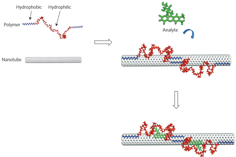
Schematic of the molecular recognition concept. A polymer with an alternating hydrophobic and hydrophilic sequence adopts a specific conformation when adsorbed to the nanotube. The polymer is pinned in place to create a selective molecular recognition site for the analyte (molecule of interest), leading to either a wavelength or intensity change in single-wall nanotube fluorescence. (Credit: Jingqing Zhang et al./Nature Nanotechnology)
Their approach takes advantage of a phenomenon that occurs when certain types of polymers bind to a carbon nanotube. These polymers, known as amphiphilic, have both hydrophobic (water-rejecting) and hydrophilic (water-accepting) regions.
These polymers are designed and synthesized such that when the polymers are exposed to carbon nanotubes, the hydrophobic regions latch onto the tubes like anchors and the hydrophilic regions form a series of loops extending away from the tubes.
These loops form a new layer surrounding the nanotube, known as a corona. The MIT researchers found that the loops within the corona are arranged very precisely along the tube, and the spacing between the anchors determines which target molecule will be able to wedge into the loops and alter the carbon nanotube’s fluorescence.
“We hope that our sensors will provide the scientific community with a new approach to detecting important molecules that is rapid and label-free,” said Markita del Carpio Landry, Ph.D., lead author, in an email interview with KurzweilAI.
“The tools required to make these sensors are relatively inexpensive and accessible, so we hope other research groups can use this technology to support their day-to-day research.
“For instance, if we can design sensors to detect molecules of clinical importance, they could be used to design technologies to sense bio-molecular markers that are indicative of diseases. Alternatively, we could design sensors to recognize hazardous molecules in our environments, such as environmental pollutants.
“Since the ability to design a sensor is only limited by our imaginations (instead of by available naturally occurring antibodies), the potential applications are equally numerous!”
The research was funded by the National Science Foundation and the Army Research Office through MIT’s Institute for Soldier Nanotechnologies.

Abstract of Nature Nanotechnology paper
Understanding molecular recognition is of fundamental importance in applications such as therapeutics, chemical catalysis and sensor design. The most common recognition motifs involve biological macromolecules such as antibodies and aptamers. The key to biorecognition consists of a unique three-dimensional structure formed by a folded and constrained bioheteropolymer that creates a binding pocket, or an interface, able to recognize a specific molecule. Here, we show that synthetic heteropolymers, once constrained onto a single-walled carbon nanotube by chemical adsorption, also form a new corona phase that exhibits highly selective recognition for specific molecules. To prove the generality of this phenomenon, we report three examples of heteropolymer-nanotube recognition complexes for riboflavin, L-thyroxine and oestradiol. In each case, the recognition was predicted using a two-dimensional thermodynamic model of surface interactions in which the dissociation constants can be tuned by perturbing the chemical structure of the heteropolymer. Moreover, these complexes can be used as new types of spatiotemporal sensors based on modulation of the carbon nanotube photoemission in the near-infrared, as we show by tracking riboflavin diffusion in murine macrophages.

(¯`*• Global Source and/or more resources at http://goo.gl/zvSV7 │ www.Future-Observatory.blogspot.com and on LinkeIn Group's "Becoming Aware of the Futures" at http://goo.gl/8qKBbK │ @SciCzar │ Point of Contact: www.linkedin.com/in/AndresAgostini

Self-soldering nanotubes could replace silicon transistors for flexible electronics

November 27, 2013
University of Illinois researchers have developed a way to solder (connect) carbon nanotubes, which are too small for even the world’s tiniest soldering iron.
Researchers have been exploring using carbon nanotubes as transistors instead of traditional silicon, because they are easier to transport onto alternate substrates, such as thin sheets of plastic, for low-cost flexible electronics or flat-panel displays.
Carbon nanotubes are high-quality conductors, but creating single tubes suitable to serve as transistors is very difficult. Arrays of nanotubes are much easier to make, but the current has to hop through junctions from one nanotube to the next, slowing it down. In standard electrical wires, such junctions would be soldered, but how could the gaps be bridged on such a small scale?
Hot-wiring a nanotube
“It occurred to me that these nanotube junctions will get hot when you pass current through them,” said  electrical and computer engineering professor Joseph Lyding, “kind of like faulty wiring in a home can create hot spots. In our case, we use these hot spots to trigger a local chemical reaction that deposits metal that nano-solders the junctions.”
The nano-soldering process is simple and self-regulating (see video). It takes only seconds and improves the device performance by an order of magnitude — almost to the level of devices made from single nanotubes, but much easier to manufacture on a large scale, he said.
[+]
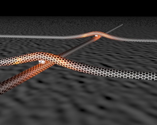
1. A carbon nanotube array is placed in a chamber pumped full of the metal-containing gas molecules. When a current passes through the transistor, the junctions heat because of resistance as electrons flow from one nanotube to the next. (Credit: Joseph W. Lyding/University of Illinois)
[+]
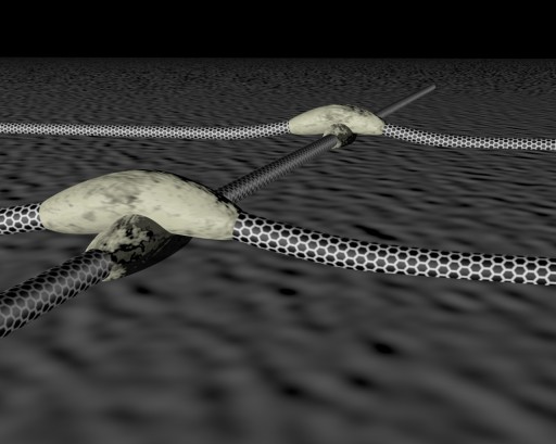
2. The molecules react to the heat, depositing the metal at the hot spots and effectively “soldering” the junctions. Then the resistance drops, as well as the temperature, so the reaction stops. (Credit: Joseph W. Lyding/University of Illinois)
[+]
3. Final result: fully metallized nanotube-nanotube junctions (credit: Joseph W. Lyding/University of Illinois)
Nanotube-based computer chips
“It would be easy to insert the CVD [chemical vapor deposition] process in existing process flows,” Lyding said. “CVD technology is commercially available off-the-shelf. People can fabricate these transistors with the ability to turn them on so that this process can be done. Then when it’s finished they can finish the wiring and connect them into the circuits. Ultimately it would be a low-cost procedure.”
“Other methods have been developed to address the nanotube junction resistance problem, but they are generally top-down and quite slow,” Lyding told KurzweilAI. “Our method is self-aligned and self-limiting and is therefore easily implemented.”
The method is easy to implement and could even be used to create complete computer chips, he said. “We are probably looking at one to three years for commercial applications that incorporate our process.”
The National Science Foundation and the Office of Naval Research supported this work.

1. What are the practical uses of this innovation?
“Transistors fabricated from arrays of carbon nanotubes are potentially low-cost, easy to fabricate and compatible with flexible substrates. Innovations, such as the striping technique developed by  John Rogers [Swanlund professor in materials science and engineering] et al. (Nature 454, 495 (2008)) demonstrate these factors while eliminating the unwanted percolation pathways of naturally occurring metallic nanotubes.
A remaining problem with these devices, however, is the high nanotube-nanotube junction resistance, which adds to power dissipation and reduces switching speed by an order of magnitude or more. The work that we have just reported reduces this nanotube-nanotube junction resistance and improves device operation (speed) by about an order of magnitude. We expect the practical uses of this innovation to be in any nanotube-based device that has nanotube-nanotube junctions.
3. How does this innovation compare to others?
researcher Joseph W. Lyding, a professor of electrical and computer engineering at the University of Illinois, explained to KurzweilAI.

Abstract of Nano Letters paper
The performance of carbon nanotube network (CNN) devices is usually limited by the high resistance of individual nanotube junctions (NJs). We present a novel method to reduce this resistance through a nanoscale chemical vapor deposition (CVD) process. By passing current through the devices in the presence of a gaseous CVD precursor, localized nanoscale Joule heating induced at the NJs stimulates the selective and self-limiting deposition of metallic nanosolder. The effectiveness of this nanosoldering process depends on the work function of the deposited metal (here Pd or HfB2), and it can improve the on/off current ratio of a CNN device by nearly an order of magnitude. This nanosoldering technique could also be applied to other device types where nanoscale resistance components limit overall device performance.


(¯`*• Global Source and/or more resources at http://goo.gl/zvSV7 │ www.Future-Observatory.blogspot.com and on LinkeIn Group's "Becoming Aware of the Futures" at http://goo.gl/8qKBbK │ @SciCzar │ Point of Contact: www.linkedin.com/in/AndresAgostini

Tuesday, November 26, 2013

FDA orders 23andMe to halt sales of its its Saliva Collection Kit and Personal Genome Service

November 26, 2013
[+]
(Credit: 23andMe Inc.)
The FDA has told 23andMe Inc., the Google Inc.-backed DNA analysis company co-founded by Anne Wojcicki, to halt sales of its Saliva Collection Kit and Personal Genome Service (PGS).
In a letter, the FDA said the company was acting “without marketing clearance or approval in violation of the Federal Food, Drug and Cosmetic Act (the FD&C Act)….”
“Most of the intended uses for PGS listed on your website, a list that has grown over time, are medical device uses [that] have not been classified and thus require premarket approval or de novo classification.”
“We recognize that we have not met the FDA’s expectations regarding timeline and communication regarding our submission,” 23andMe responded in a statement. “Our relationship with the FDA is extremely important to us and we are committed to fully engaging with them to address their concerns.”
With more than 500,000 genotyped customers, 23andMe enables individuals to gain deeper insights into personal ancestry, genealogy and inherited traits. It offers $99 saliva-testing kits that customers can use at home and then send to the company for reports on how they might be at risk for a range of inherited health conditions and how they are likely to respond to certain drugs.


(¯`*• Global Source and/or more resources at http://goo.gl/zvSV7 │ www.Future-Observatory.blogspot.com and on LinkeIn Group's "Becoming Aware of the Futures" at http://goo.gl/8qKBbK │ @SciCzar │ Point of Contact: www.linkedin.com/in/AndresAgostini

Berkeley Lab scientists record first inside look at carbon-capture molecular structure

November 26, 2013
[+]
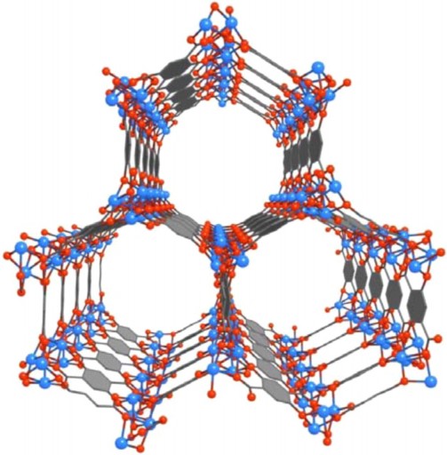
Mg-MOF-74 is a metal-organic framework (MOF) whose porous crystalline structure could enable it to serve as a storage vessel for capturing and containing the carbon dioxide emitted from coal-burning power plants (credit: National Academy of Sciences)
Researchers with Lawrence Berkeley National Laboratory (Berkeley Lab) have recorded the first electronic structure observations of the adsorption of carbon dioxide inside a metal-organic framework (MOF).
The “Mg-MOF-74″ MOF’s porous crystalline structure could enable it to serve as a storage vessel for capturing and containing the carbon dioxide emitted from coal-burning power plants.
MOFs are molecular systems consisting of a metal oxide center surrounded by organic “linker” molecules that form a highly porous three-dimensional crystal framework.
This microporous crystal structure enables MOFs to serve as storage vessels with a sponge-like capacity for capturing and containing carbon dioxide, thought to be one of the primary greenhouse gases responsible for exacerbating global climate change.
When a solvent molecule applied during the formation of the MOF is subsequently removed, the result is an unsaturated “open” metal site MOF that has a strong affinity for carbon dioxide.
Working at Berkeley Lab’s Advanced Light Source (ALS), a team led by Jeff Kortright of Berkeley Lab’s Materials Sciences Division used the X-ray spectroscopy technique known as Near Edge X-ray Absorption Fine Structure (NEXAFS) to obtain what are believed to be the first ever measurements of chemical and electronic signatures inside of a MOF during gas adsorption.
[+]
Advanced Light Source (credit: Berkeley Lab)
“Open metal site MOFs preferentially adsorb carbon dioxide over nitrogen or methane due to carbon dioxide’s larger quadrupole moment and greater polarizability,” Kortright says. “Mg-MOF-74 with its unique pyramidal geometry is especially selective for carbon dioxide over other greenhouse gases and has an exceptionally large storage capacity.”
Support for this work was provided by the Center for Gas Separations Relevant to Clean Energy Technologies, an Energy Frontier Research Center funded by the DOE Office of Science.

Abstract of Journal of the American Chemical Society paper
We explore the local electronic signatures of molecular adsorption at coordinatively unsaturated binding sites in the metal–organic framework Mg-MOF-74 using X-ray spectroscopy and first-principles calculations. In situ measurements at the Mg K-edge reveal distinct pre-edge absorption features associated with the unique, open coordination of the Mg sites which are suppressed upon adsorption of CO2 and N,N′-dimethylformamide. Density functional theory shows that these spectral changes arise from modifications of local symmetry around the Mg sites upon gas uptake and are strongly dependent on the metal–adsorbate binding strength. The expanded MOF Mg2(dobpdc) displays the same behavior upon adsorption of CO2 and N,N′-dimethylethylenediamine. Similar sensitivity to local symmetry is expected for any open metal site, making X-ray spectroscopy an ideal tool for examining adsorption in such MOFs. Qualitative agreement between ambient-temperature experimental and 0 K theoretical spectra is good, with minor discrepancies thought to result from framework vibrational motion.


(¯`*• Global Source and/or more resources at http://goo.gl/zvSV7 │ www.Future-Observatory.blogspot.com and on LinkeIn Group's "Becoming Aware of the Futures" at http://goo.gl/8qKBbK │ @SciCzar │ Point of Contact: www.linkedin.com/in/AndresAgostini

A patient-specific 3D virtual birth simulator

November 26, 2013
uea_virtual_childbirth
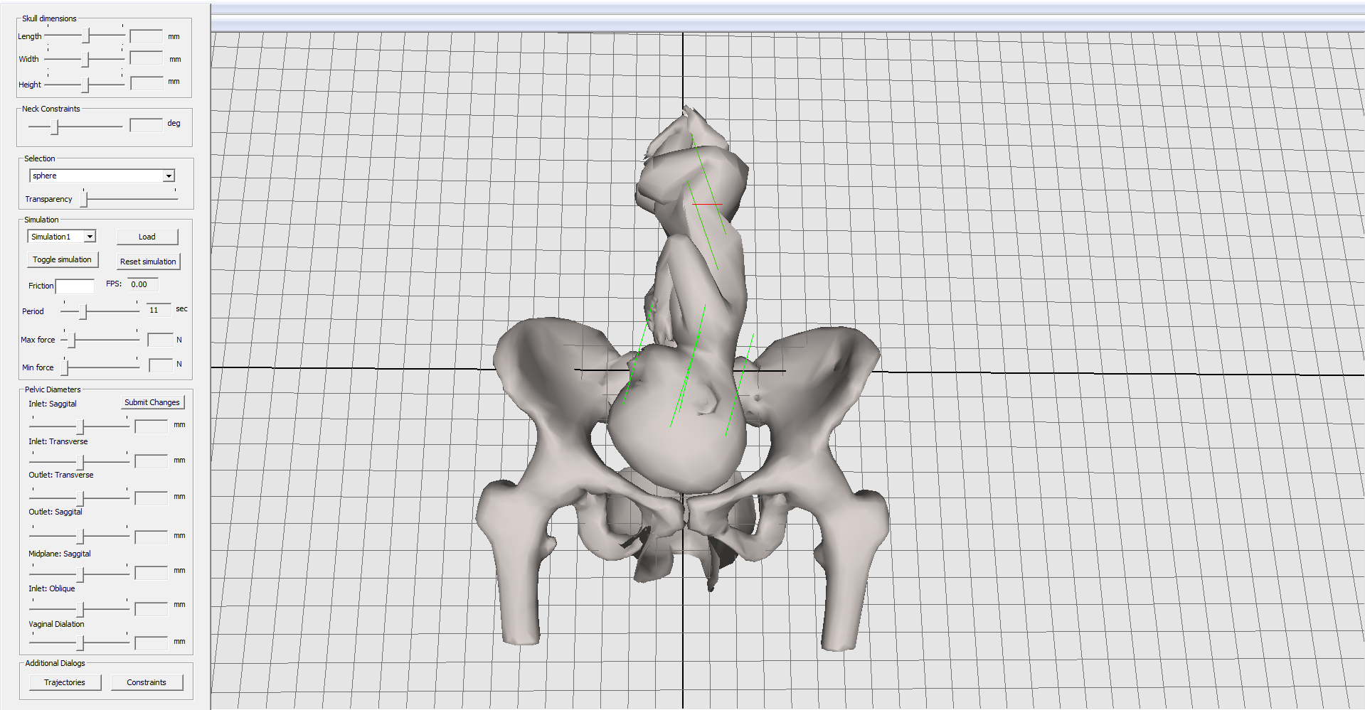
User interface of the current version of the childbirth simulator (credit: University of East Anglia)
Computer scientists from the University of East Anglia are developing a virtual birthing simulator that will help doctors and midwives prepare for unusual or dangerous births.
The new program will take into account factors such as the shape of the mother’s body and the positioning of the baby to provide patient-specific birth predictions.
“We are creating a … simulation of childbirth using 3D graphics to simulate the sequence of movements as a baby descends through the pelvis during labor,” said Dr. Rudy Lapeer from UEA’s school of Computing Sciences, who is leading the project.
“Users will be able to input key anatomical data — such as the size and shape of the mother’s pelvis, and the baby’s head and torso. By doing this you will be able to set different bespoke [custom] scenarios for both the mother and baby.”
[+]
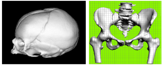
Geometric models of a fetal skull and maternal pelvis (credit: University of East Anglia)
Ultrasound data is used to re-create a geometric model of a baby’s skull and body in 3D graphics as well as the mother’s body and pelvis.
Programmers are also taking into account the force from the mother pushing during labor and are modeling a virtual midwife’s hands interacting with the baby’s head.
“Because this program is patient-specific, doctors and midwives will be able to see how a birth may take place before it has happened on a case-by-case basis. For example, you would be able to see if a baby’s shoulders will get stuck.
“We hope that this could help to avoid complicated births altogether by guiding people in the medical profession to advise on caesarean sections where necessary.”

Abstract of IEEE International Conference on E-Health and Bioengineering paper
The paper presents initial experiments on a basic forward engineered childbirth simulator. Polygonal models of a fetal skull and bony maternal pelvis were created. A simple physics model was implemented to model the mechanical contact interaction between the fetal head and the maternal pelvis. A series of experiments were run to establish whether this basic model would display the cardinal movements which are observed during normal labour. Though the first three movements were observed without needing reverse engineered action, the subsequent cardinal movements required the use of waypoints along the trajectory of the birth canal. It was concluded that more complex geometry, including a fully articulated fetus and the inclusion of soft tissue would be required to arrive at a realistic fully functional forward engineered human childbirth simulator.


(¯`*• Global Source and/or more resources at http://goo.gl/zvSV7 │ www.Future-Observatory.blogspot.com and on LinkeIn Group's "Becoming Aware of the Futures" at http://goo.gl/8qKBbK │ @SciCzar │ Point of Contact: www.linkedin.com/in/AndresAgostini

Steering toxic drug-filled nanoparticles to zap cancer, not healthy cells

November 26, 2013
nanoparticles_magnasim
Artist’s impression of drug-filled mag­netic nanopar­ti­cle (credit: Northeastern Magnasim team)
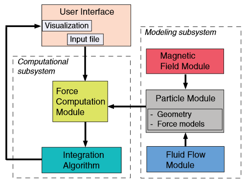
North­eastern researchers are developing sim­u­la­tion soft­ware called Mag­nasim to more accu­rately steer simulated drug-filled mag­netic nanopar­ti­cles to tumor masses where they can safely dis­charge their con­tents.
[+]
Magnasim software architecture (credit: P. Vartholomeos et al./IEEE Transactions on Biomedical Engineering)
The drugs used to kill cancer cells are just as toxic to neigh­boring healthy cells, so researchers have long sought a drug delivery method that tar­gets only cancer cells, bypassing the healthy ones.
Func­tional Mag­netic Res­o­nance Imaging (fMRI) is being used clinically to guide drug-filled mag­netic nanopar­ti­cles, but con­trol­ling their course accurately is still more an art than a sci­ence, said Dinos Mavroidis, Dis­tin­guished Pro­fessor of Mechan­ical and Indus­trial Engi­neering at North­eastern.
“There are only a few groups worldwide that are working on targeted drug delivery using magnetic fields,” Mavroidis explained to KurzweilAI. “We are collaborating with most of them. So far there is no commercial product on the market for targeted drug delivery using magnetic fields or for the simulation software. We expect the Mag­nasim software to be on the market in 1–2 years.”
Full disclosure: I was formerly a member of a research team at Biophan Technologies, Inc. developing technologies to guide drug-filled mag­netic nanopar­ti­cles, but I have no current financial interests aside from a small amount of stock. — Amara D. Angelica, Editor

Abstract of IEEE Transactions on Biomedical Engineering paper
A computational platform has been developed to perform simulation, visualization, and postprocessing analysis of the aggregation process of magnetic particles within a fluid environment such as small arteries and arterioles or fluid-filled cavities of the human body. The mathematical models needed to describe the physics of the system are presented in detail and also computational algorithms needed for efficient computation of these models are described. A number of simulation results demonstrate the simulation capabilities of the platform and preliminary experimental results validate simulation predictions. The platform can be used to design optimal strategies for magnetic steering and magnetic targeting of drug-loaded magnetic microparticles.
Abstract of Annual Reviews Biomedical Engineering paper
[+]
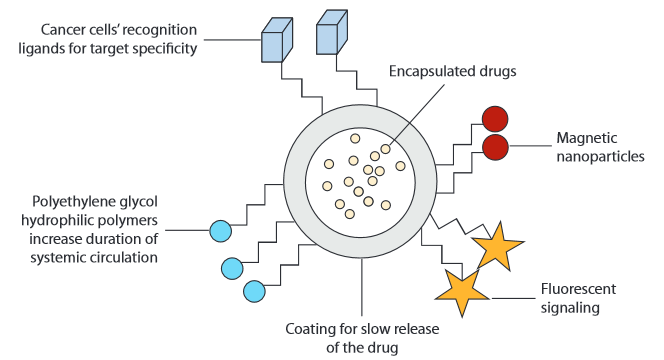
Multifunctionalized drug-loaded nanoparticle (credit: P. Vartholomeos et al./Annual Reviews Biomedical Engineering)
This review presents the state of the art of magnetic resonance imaging (MRI)-guided nanorobotic systems that can perform diagnostic, curative, and reconstructive treatments in the human body at the cellular and subcellular levels in a controllable manner.
The concept of an MRI-guided nanorobotic system is based on the use of an MRI scanner to induce the required external driving forces to propel magnetic nanocapsules to a specific target.
It is an active targeting mechanism that provides simultaneous propulsion and imaging capabilities, which allow the implementation of real-time feedback control of the targeting process. The architecture of the system comprises four main modules: (a) the nanocapsules, (b) the MRI propulsion module, (c) the MRI tracking module (for image processing), and (d) the controller module.
A key concept is the nanocapsule technology, which is based on carriers such as liposomes, polymer micelles, gold nanoparticles, quantum dots, metallic nanoshells, and carbon nanotubes. Descriptions of the significant challenges faced by the MRI-guided nanorobotic system are presented, and promising solutions proposed by the involved research community are discussed. Emphasis is placed on reviewing the limitations imposed by the scaling effects that dominate within the blood vessels and also on reviewing the control algorithms and computational tools that have been developed for real-time propulsion and tracking of the nanocapsules.


(¯`*• Global Source and/or more resources at http://goo.gl/zvSV7 │ www.Future-Observatory.blogspot.com and on LinkeIn Group's "Becoming Aware of the Futures" at http://goo.gl/8qKBbK │ @SciCzar │ Point of Contact: www.linkedin.com/in/AndresAgostini

Monday, November 25, 2013

Will 2D tin be the next super material for chip interconnects?

New single-layer material could go beyond graphene, conducting electricity with 100 percent efficiency at room temperature
November 25, 2013
[+]
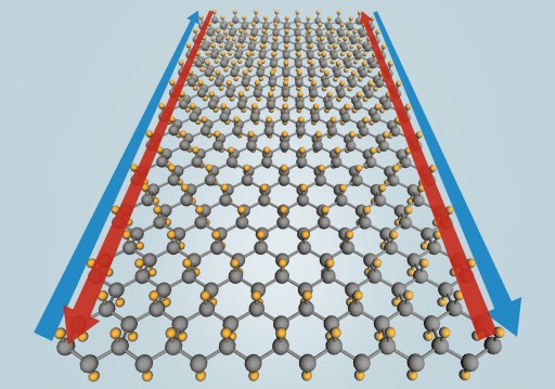
Adding fluorine atoms (yellow) to a single layer of tin atoms (grsy) should allow a predicted new material, stanene, to conduct electricity perfectly along its edges (blue and red arrows) at temperatures up to 100 degrees Celsius (212 Fahrenheit) (credit: Yong Xu/Tsinghua University; Greg Stewart/SLAC)
Move over, graphene. “Stanene” —  a single layer of tin atoms — could be the world’s first material to conduct electricity with 100 percent efficiency at the temperatures that computer chips operate, according to a team of theoretical physicists led by researchers from the U.S. Department of Energy’s (DOE) SLAC National Accelerator Laboratory and Stanford University.
Stanene — the Latin name for tin (stannum) combined with the suffix used in graphene —  could “increase the speed and lower the power needs of future generations of computer chips, if our prediction is confirmed by experiments that are underway in several laboratories around the world,” said team leader Shoucheng Zhang, a physics professor at Stanford and the Stanford Institute for Materials and Energy Sciences (SIMES), a joint institute with SLAC.
For the past decade, Zhang and colleagues have been calculating and predicting the electronic properties of a special class of materials known as topological insulators, which conduct electricity only on their outside edges or surfaces and not through their interiors. When topological insulators are just one atom thick, their edges conduct electricity with 100 percent efficiency. These unusual properties result from complex interactions between the electrons and nuclei of heavy atoms in the materials.
Their calculations indicated that a single layer of tin would be a topological insulator at and above room temperature, and that adding fluorine atoms to the tin would extend its operating range to at least 100 degrees Celsius (212 degrees Fahrenheit).
Ultimately a silicon substitute?
Zhang said the first application for this stanene-fluorine combination could be for interconnects — wiring that connects the many sections of a microprocessor — allowing electrons to flow as freely as cars on a highway. Traffic congestion would still occur at on- and off-ramps made of conventional conductors, he said. But stanene wiring should significantly reduce the power consumption and heat production of microprocessors.
Manufacturing challenges include ensuring that only a single layer of tin is deposited and keeping that single layer intact during high-temperature chip-making processes.
“Eventually, we can imagine stanene being used for many more circuit structures, including replacing silicon in the hearts of transistors,” Zhang said.
Additional contributors included researchers from Tsinghua University in Beijing and the Max Planck Institute for Chemical Physics of Solids in Dresden, Germany. The research was supported by the Mesodynamic Architectures program of the Defense Advanced Research Projects Agency.

Abstract of Physical Review Letters paper
The search for large-gap quantum spin Hall (QSH) insulators and effective approaches to tune QSH states is important for both fundamental and practical interests. Based on first-principles calculations we find two-dimensional tin films are QSH insulators with sizable bulk gaps of 0.3 eV, sufficiently large for practical applications at room temperature. These QSH states can be effectively tuned by chemical functionalization and by external strain. The mechanism for the QSH effect in this system is band inversion at the Γ point, similar to the case of a HgTe quantum well. With surface doping of magnetic elements, the quantum anomalous Hall effect could also be realized.


(¯`*• Global Source and/or more resources at http://goo.gl/zvSV7 │ www.Future-Observatory.blogspot.com and on LinkeIn Group's "Becoming Aware of the Futures" at http://goo.gl/8qKBbK │ @SciCzar │ Point of Contact: www.linkedin.com/in/AndresAgostini

Ultrasound-released nanoparticles may help diabetics avoid the needle

November 25, 2013
[+]
New technique allows diabetics to control insulin release with an injectable nano-network and portable ultrasound device (credit: NCSU)
A new nanotechnology-based technique for regulating blood sugar in diabetics could give patients the ability to release insulin painlessly using a small ultrasound device, allowing them to go days between injections — rather than using needles to give themselves multiple insulin injections each day.
A patient who has type 1 or advanced type 2 diabetes needs additional insulin, a hormone that transports glucose — or blood sugar — from the bloodstream into the body’s cells.
These diabetes patients must inject insulin as needed to ensure their blood sugar levels are in the “normal” range. However, these injections can be painful.
The new technique — developed by Dr. Zhen Gu,  an assistant professor in the joint biomedical engineering program at NC State and UNC-Chapel Hill, and other researchers at North Carolina State University and the University of North Carolina at Chapel Hill — may offer a solution.
[+]
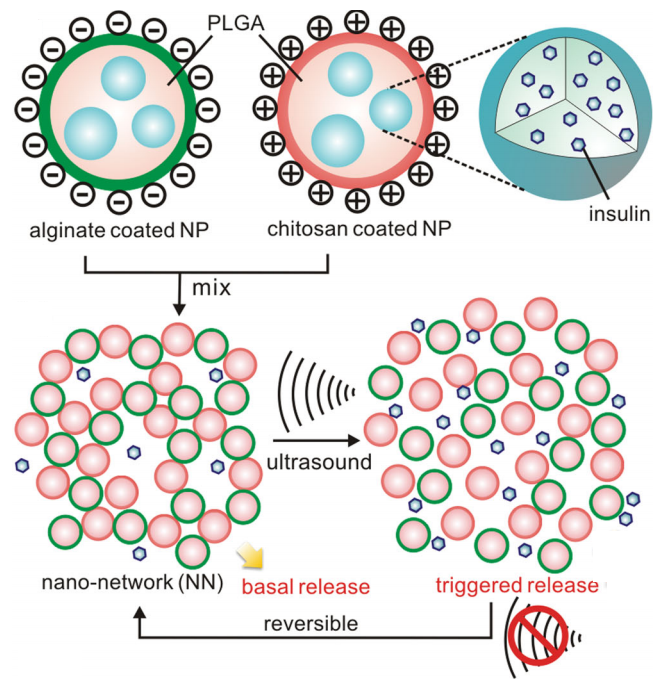
Insulin delivery system (credit: Di et al./Advanced Healthcare Materials)
How the insulin delivery system works
1. Biocompatible and biodegradable nanoparticles are injected into a patient’s skin. The nanoparticles are made out of poly(lactic-co-glycolic) acid (PLGA) and are filled with insulin.
(Each of the PLGA nanoparticles is given either a positively charged coating made of chitosan (a biocompatible material normally found in shrimp shells), or a negatively charged coating made of alginate (a biocompatible material normally found in seaweed). When the solution of coated nanoparticles is mixed together, the positively and negatively charged coatings are attracted to each other by electrostatic force to form a “nano-network.”)
2. Once injected into the subcutaneous layer of the skin, that nano-network holds the nanoparticles together and prevents them from dispersing throughout the body.
3. The injected insulin begins to diffuse from the  coated PLGA nanoparticles, which are also porous. But most of the insulin doesn’t stray far — it is suspended in a de facto reservoir in the subcutaneous layer of the skin by the electrostatic force of the nano-network. This essentially creates a dose of insulin that is simply waiting to be delivered into the bloodstream.
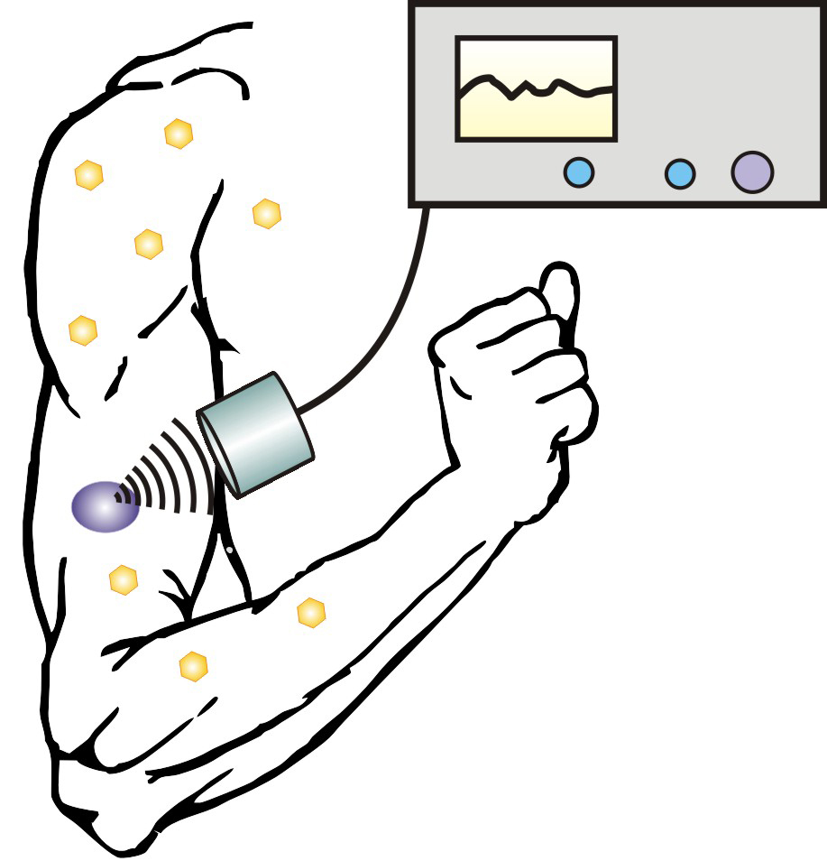
4. The patient can use a small, hand-held device to apply focused ultrasound waves to the site of the nano-network, painlessly releasing the insulin from its de facto reservoir into the bloodstream.
When the ultrasound is removed, the electrostatic force reasserts itself and pulls the nanoparticles in the nano-network back together. The nanoparticles then diffuse more insulin, refilling the reservoir.
5. When the insulin runs out, a new nano-network has to be injected.
Ultrasonic waves generate microscope gas bubbles

The researchers believe the technique works because the ultrasound waves excite microscopic gas bubbles in the tissue, temporarily disrupting the nano-network in the subcutaneous layer of the skin. That disruption pushes the nanoparticles apart, relaxing the electrostatic force being exerted on the insulin in the reservoir.
This allows the insulin to begin entering the bloodstream — a process hastened by the effect of the ultrasound waves pushing on the insulin.
“We know this technique works, and we think this is how it works, but we are still trying to determine the precise details,” says Dr. Yun Jing, an assistant professor of mechanical engineering at NC State and co-corresponding author of the paper.
“We’ve done proof-of-concept testing in laboratory mice with type 1 diabetes,” Gu says. “We found that this technique achieves a quick release of insulin into the bloodstream, and that the nano-networks contain enough insulin to regulate blood glucose levels for up to 10 days.”
“The system may be available commercially in a few years, but we first need to perform large animal studies and clinical trials, Gu told KurzweilAI. Gu is also a senior author of a paper on the research.
“Compared to the traditional insulin delivery method (needle/syringe based), our method is non-invasive, painless, with quick response. and can last a long time (one injection can last over a week, or even longer),” he said.
This work was supported by NC TraCS, NIH’s Clinical and Translational Science Awards at UNC-CH.

Abstract of Advanced Healthcare Materials paper
An on demand, non-invasive and portable insulin delivery method that can achieve pulsatile insulin release and effective regulation of blood glucose is highly desirable for type 1 and advanced type 2 diabetes administration. We report that integration of an injectable nano-network with a focused ultrasound system (FUS) can remotely regulate insulin release both in vitro and in vivo. Serving as a synthetic insulin reservoir, the nano-network consisting of adhesive poly(lactic-co-glycolic acid)  nanoparticles significantly promoted insulin release upon intermittent FUS triggers. Remarkably, a maximum of 80-fold increase in the insulin release rate was observed when the nano-network was exposed to the irradiation of ultrasound for 30 sec. In vivo studies validated that this method provided repeatable and spatiotemporal regulation of blood glucose levels in Type 1 diabetic mice. A single subcutaneous injection of the nano-network with intermittent FUS administration facilitated reduction of the blood glucose levels for up to 10 days.


(¯`*• Global Source and/or more resources at http://goo.gl/zvSV7 │ www.Future-Observatory.blogspot.com and on LinkeIn Group's "Becoming Aware of the Futures" at http://goo.gl/8qKBbK │ @SciCzar │ Point of Contact: www.linkedin.com/in/AndresAgostini

Black hole birth captured by ‘armada of instruments’

"A Rosetta-Stone event ... may require physicists to modify existing theories about radiation"
November 25, 2013
star_becomes_black_hole
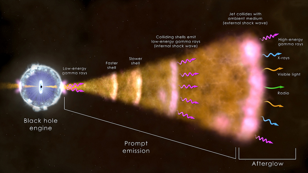
An artist’s conception of the processes by which a star collapses and becomes a black hole, releasing high-energy gamma rays and X-rays, as well as visible light, in the process (credit: NASA)
“Los Alamos’ RAPTOR telescopes in New Mexico and Hawaii received a very bright cosmic birth announcement for a black hole on April 27,” said astrophysicist Tom Vestrand, lead author of a paper n the journal Science Nov. 21 that highlights the unusual event.
“This was the burst of the century,” said Los Alamos co-author James Wren. “It’s the biggest, brightest one to happen in at least 20 years, and maybe even longer than that.”
The RAPTOR (RAPid Telescopes for Optical Response) system — designed by Los Alamos National Laboratory — is a network of small robotic observatories that scan the skies for optical anomalies such as flashes emanating from a star in its death throes as it collapses and becomes a black hole, an object so dense that not even light can escape its gravity field.
This flash — optical light generated simultaneously with x-rays and gamma rays during a gamma ray burst (GRB) — provides clues about the nature of the explosions that occur as massive stars collapse. It arrived from the constellation Leo in the form of an exceptionally bright flash of visible light that accompanied a powerful burst of cosmic gamma-ray emissions. It lasted about 80 seconds before it faded below the ~10th magnitude sensitivity limit of the RAPTOR full sky monitors.
Witnessed by an armada of instruments
What made such an extremely rare event even more spectacular for scientists, however, is that, in addition to the RAPTOR sighting, it was witnessed by an armada of instruments — including gamma-ray and X-ray detectors aboard NASA’s Fermi, NuSTAR and Swift satellites. While the NASA instruments recorded some of the highest-energy gamma-ray bursts ever measured from such an event, RAPTOR noticed that the massive and violent transformation of a star into a black hole yielded a lingering “afterglow” that faded in lock-step with the highest energy gamma-rays.
“This afterglow is interesting to see,” said paper co-author Przemek Wozniak of Los Alamos’s Intelligence and Space Research Division. “We normally see a flash associated with the beginning of an event, analogous to the bright flash that you would see coinciding with the explosion of a firecracker. This afterglow may be somewhat analogous to the embers that you might be able to see lingering after your firecracker has exploded. It is the link between the optical phenomenon and the gamma-rays that we haven’t seen before, and that’s what makes this display extremely exciting.”
A Rosetta-Stone event
The event was among the brightest and most energetic of its type ever witnessed. “This was a Rosetta-Stone event that illuminates so many things — literally,” Vestrand said. “We were very fortunate to have all of the NASA and ground-based instruments seeing it at the same time. We had all the assets in place to collect a very detailed data set. These are data that astrophysicists will be looking at for a long time to come because we have a detailed record of the event as it unfolded.”
Already the event, labeled GRB 130427A by astrophysicists, is testing some long-held assumptions about the nature of the universe. For example, scientists recorded energy levels for gamma rays that are higher than what some researchers thought theoretically possible. This revelation may require physicists to modify existing theories about radiation. No doubt, the data set could yield more surprises in the future, Vestrand said.
Other organizations affiliated with the research include Stanford University, the University of Alabama, Las Cumbres Observatory Global Telescope Network and the Universities Space Research Association.

Abstract of Science paper
The optical light generated simultaneously with x-rays and gamma-rays during a gamma-ray burst (GRB) provides clues about the nature of the explosions that occur as massive stars collapse. We report on the bright optical flash and fading afterglow from powerful burst GRB 130427A. The optical and >100 MeV gamma-ray flux show a close correlation during the first 7000 s, best explained by reverse shock emission co-generated in the relativistic burst ejecta as it collides with surrounding material. At later times, optical observations show the emergence of emission generated by a forward shock traversing the circumburst environment. The link between optical afterglow and >100 MeV emission suggests that nearby early peaked afterglows will be the best candidates for studying particle acceleration at GeV/TeV energies.


(¯`*• Global Source and/or more resources at http://goo.gl/zvSV7 │ www.Future-Observatory.blogspot.com and on LinkeIn Group's "Becoming Aware of the Futures" at http://goo.gl/8qKBbK │ @SciCzar │ Point of Contact: www.linkedin.com/in/AndresAgostini

FDA allows marketing of ‘next generation’ gene-sequencing devices

A boost for personalized medicine and pharmocogenomics
November 25, 2013
MiSeq Benchtop Sequencer (credit: Illumina)
The FDA has approved marketing of four diagnostic devices from Illumina (a manufacturer of DNA sequencing machines) for “next generation sequencing” (NGS) — meaning the devices can now quickly and cheaply read and interpret large segments of the genome (the set of genetic information in your body) in a single test.
Two of the devices allow laboratories to sequence a patient’s genome for any purpose, according to Jeffrey Shuren, M.D., Director of FDA’s Center for Devices and Radiological Health in an FDA blog.
“The software compares the patient’s sequence to a normal human genome sequence used for reference and identifies the differences.”
The other two devices can only detect changes in the CFTR gene, which can result in cystic fibrosis, a disease inherited through a faulty CFTR gene from both parents. (More than 10 million Americans are carriers of cystic fibrosis.)
One of these tests could identify men and women with the faulty CFTR gene; the second test looks for other, perhaps unexpected, mutations in the CFTR gene that could be having an impact on the patient’s health, Shuren said.
Personalized medicine and pharmacogenomics
Based on this FDA decision, “clinicians can now selectively look for an almost unlimited number of genetic changes that may be of medical significance,” National Institutes of Health head Francis Collins and FDA head Margaret Hamburg write in an editorial in the New England Journal of Medicine (open access).
For example, “patients diagnosed with a cancer for which there are few therapeutic options may … benefit from drug therapies originally aimed at other cancers that share common driver mutations.”
What happens when your entire genomic information is in your electronic medical record, they suggest? So instead of having to take a DNA sample, ship it, and wait for a lab to run a test, only a quick electronic query would provide your physician with the needed information to determine the course of treatment. That includes pharmacogenomics — the use of genomic information to identify the right drug at the right dose for each patient.
But Collins and Hamburg also caution that new genomic findings need to be validated before they can be integrated into medical decision making. “Doctors and other health care professionals will need support in interpreting genomic data and their meaning for individual patients. Patients will want to be able to talk about their genetic information with their doctor.. and participate alongside their doctors in making more informed decisions.”
That all sounds great, but what happens when non-medically trained Affordable Care Act “navigators” and flakey, hacker-prone medical insurance information systems (like the disastrous kludge for ACA developed by NIH) get access to this highly sensitive information? — Editor


(¯`*• Global Source and/or more resources at http://goo.gl/zvSV7 │ www.Future-Observatory.blogspot.com and on LinkeIn Group's "Becoming Aware of the Futures" at http://goo.gl/8qKBbK │ @SciCzar │ Point of Contact: www.linkedin.com/in/AndresAgostini

Friday, November 22, 2013

3D-printing multi-material objects in minutes instead of hours

November 22, 2013
[+]
A computer model of a pair of tweezers shows the distribution of materials and degrees of hardness in the object to be 3-D printed in Dr. Yong Chen’s lab at USC Viterbi (credit: USC Viterbi)
In another leap for 3D printing, researchers at the USC Viterbi School of Engineering have developed a faster 3D printing process that allows for 3D-printing multi-material objects in minutes instead of hours.
Fabrication time and the complexity of multi-material objects have been a hurdle to widespread use of 3D printing.
Speeding up printing
USC Viterbi researchers developed improved mask-image-projection-based stereolithography (MIP-SL) to drastically speed up the fabrication of homogeneous 3D objects. In the MIP-SL process, a 3D digital model of an object is sliced by a set of horizontal planes and each slice is converted into a two-dimensional mask image.
[+]
Heterogeneous model. Left: the CAD model; right: the fabricated part. (Credit: Zhou C. et al./Rapid Prototyping Journal)
The mask image is then projected onto a photocurable liquid resin surface and light is projected onto the resin to cure it in the shape of the related layer.
The USC Viterbi team also developed a two-way movement design for bottom-up projection so that the resin could be quickly spread into uniform thin layers. As a result, production time was cut from hours to a few minutes.
[+]
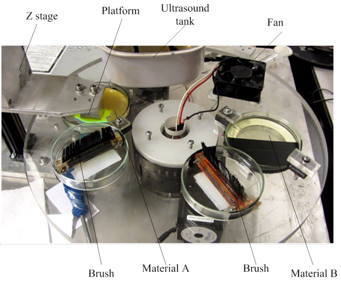
Rotary fabrication system for printing two materials per layer, including cleaning (credit: USC Viterbi)
Multi-material objects
In their latest paper, the team successfully applies this more efficient process to the fabrication of heterogeneous objects (which comprise different materials that cure at different rates).
This new 3D printing process will allow for dental and robotics models, for example, to be fabricated more cost- and time-efficiently than ever before.
“Multi-material printers are commercially available from Stratasys (Objet Connex).  However, only limited materials (photocurable resins) can be used since liquid resins need to pass through small nozzles. Our approach may expand the selections of base materials that are used in multi-material printing,” Chen explained to KurzweilAI.
“Our system provides more design freedoms for product designers and may enable them to design components with better performance or multi-functions,” Daniel J. Epstein, Department of Industrial and Systems Engineering and the study’s lead researcher, added.
“It is still in the research phase.  We will actively commercialize it through licensing to existing companies or creating a new company in the future.”
Chen his team next plan to investigate how to develop an automatic design approach for heterogeneous material distribution for user-specified physical properties and how to improve the fabrication speed.
The study was partially supported by the National Science Foundation.


(¯`*• Global Source and/or more resources at http://goo.gl/zvSV7 │ www.Future-Observatory.blogspot.com and on LinkeIn Group's "Becoming Aware of the Futures" at http://goo.gl/8qKBbK │ @SciCzar │ Point of Contact: www.linkedin.com/in/AndresAgostini

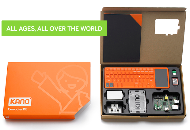
Kano: a computer anyone can make

November 22, 2013
ll_ages_over_the_world_kano
(Credit: Kano)
Kano is a computer you make yourself. Simple as Lego, powered by Pi.
What’s inside
  1. Kano Books, illustrated and intuitive
  2. Kano OS and Levels on 8GB SD card
  3. DIY Speaker
  4. Raspberry Pi Model B
  5. Kano Keyboard Combo
  6. Custom case
  7. Card mods and stencils
  8. Stickers!
  9. Cables: HDMI*, Mini-USB
  10. Smart power plug (all region pins available)
  11. WiFi powerup
[+]
“We made a computer!” (Credit: Kano Academy)
The software combines Kano OS, a distribution of Debian Linux, with an interface that feels a bit like a console game. It runs six Kano Levels, software projects to make Pong, Snake, Minecraft, videos, and music.
“Connect blocks, output Python or Javascript, and see games change before your eyes, with live code updating. Make your own power-ups (two-player-mode, teleportation) then earn new ones. Huge Pong balls! Massive TNT towers! Code cheats, beat your friends.”


(¯`*• Global Source and/or more resources at http://goo.gl/zvSV7 │ www.Future-Observatory.blogspot.com and on LinkeIn Group's "Becoming Aware of the Futures" at http://goo.gl/8qKBbK │ @SciCzar │ Point of Contact: www.linkedin.com/in/AndresAgostini

Faster, cheaper biofuel production

November 22, 2013
Thalassiosira_pseudonana
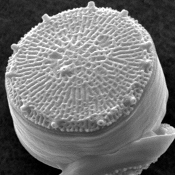
A scanning electron microscope image of the diatom Thalassiosira pseudonana (credit: Scripps Institution of Oceanography at UC San Diego)
Researchers at Scripps Institution of Oceanography at UC San Diego have developed a method for greatly enhancing biofuel production in tiny marine algae by genetically engineering a key growth component in biofuel.
The researchers say a significant roadblock in algal biofuel research surrounds the production of lipid oils, the fat molecules that store energy that can be produced for fuel: algae mainly produce the desired lipid oils when they are starved for nutrients.
Yet if they are limited in nutrients, they don’t grow well. With a robust diet algae grow well, but they produce carbohydrates instead of the desired lipids for fuel.
Genetically engineering diatoms
As reported in this week’s online edition of the Proceedings of the National Academy of Sciences (open access), Scripps graduate student Emily Trentacoste and her colleagues used a data set of genetic expression (called “transcriptomics” in laboratories) to target a specific enzyme inside a group of microscopic algae known as diatoms (Thalassiosira pseudonana).
By metabolically engineering a “knock-down” of fat-reducing enzymes called lipases, the researchers were able to increase lipids (oils) without compromising growth. The genetically altered strains they developed, the researchers say, could be produced broadly in other species.
“These results demonstrate that targeted metabolic manipulations can be used to increase accumulation of fuel-relevant molecules, with no negative effects on growth,” said Trentacoste. “We have shown that engineering this pathway is a unique and practical approach for increasing lipid yields.”
“Scientifically this is a huge achievement,” said Mark Hildebrand, a marine biology professor at Scripps and a coauthor of the study. “Five years ago people said you would never be able to get more lipids without affecting growth negatively. This paper shows that there isn’t an intrinsic barrier and gives us hope of more new things that we can try — it opens the door to a lot more work to be done.”
Faster, cheaper   production
In addition to lowering the cost of biofuel production by increasing lipid content, the new method has led to advances in the speed of algal biofuel crop production due to the efficient screening process used in the new study.
“Maintaining high growth rates and high biomass accumulation is imperative for algal biofuel production on large economic scales,” the authors note in the paper.
“Increasing lipid accumulation in microalgae is a major priority to boost the economic viability of algal biofuels, but growth and biomass are also important characteristics in large-scale production systems,” Trentacoste told KurzweilAI. “The specific enzyme targeted in this study is conserved throughout eukaryotes, and could be targeted in other production strains as well, thus these methods could be applied to many algal biofuel systems.
“A U.S. provisional patent application has been filed in relation to this invention,” she said. “Interested licensees can contact Dr. Donald Kakuda (dkakuda@ucsd.edu) at University of California-San Diego’s Technology Transfer Office.”
The National Institutes of Health, California Energy Commission, Air Force Office of Scientific Research, Department of Energy, and National Science Foundation supported the research.

Abstract of Proceedings of the National Academy of Sciences paper
Biologically derived fuels are viable alternatives to traditional fossil fuels, and microalgae are a particularly promising source, but improvements are required throughout the production process to increase productivity and reduce cost. Metabolic engineering to increase yields of biofuel-relevant lipids in these organisms without compromising growth is an important aspect of advancing economic feasibility. We report that the targeted knockdown of a multifunctional lipase/phospholipase/acyltransferase increased lipid yields without affecting growth in the diatom Thalassiosira pseudonana. Antisense-expressing knockdown strains 1A6 and 1B1 exhibited wild-type–like growth and increased lipid content under both continuous light and alternating light/dark conditions. Strains 1A6 and 1B1, respectively, contained 2.4- and 3.3-fold higher lipid content than wild-type during exponential growth, and 4.1- and 3.2-fold higher lipid content than wild-type after 40 h of silicon starvation. Analyses of fatty acids, lipid classes, and membrane stability in the transgenic strains suggest a role for this enzyme in membrane lipid turnover and lipid homeostasis. These results demonstrate that targeted metabolic manipulations can be used to increase lipid accumulation in eukaryotic microalgae without compromising growth.


(¯`*• Global Source and/or more resources at http://goo.gl/zvSV7 │ www.Future-Observatory.blogspot.com and on LinkeIn Group's "Becoming Aware of the Futures" at http://goo.gl/8qKBbK │ @SciCzar │ Point of Contact: www.linkedin.com/in/AndresAgostini

More-realistic 3D imaging technique speeds up production of movie images, modeling human organs

November 22, 2013
anisotropic_triangles
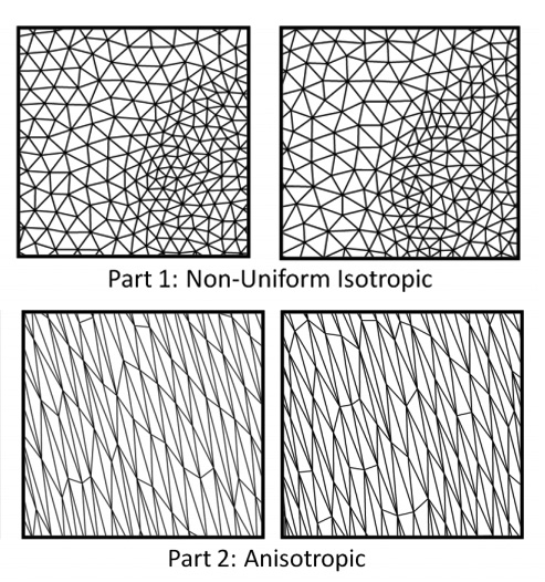
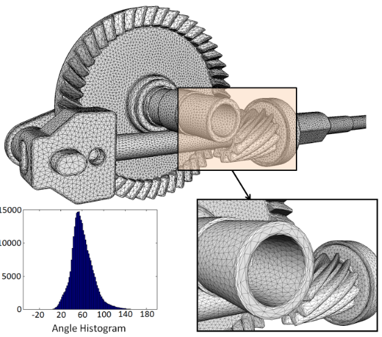
Guo and his team found that replacing isotropic triangles (part 1) with anisotropic triangles (part 2) in the particle-based method of creating images resulted in smoother representations of objects (credit: UT Dallas)
UT Dallas computer scientists have developed a technique to make 3D images faster and with more accuracy.
The method uses anisotropic (irregular) triangles — triangles with sides that vary in length depending on their direction — to create 3D “mesh” computer graphics that more accurately approximate the shapes of the original objects, and in a shorter amount of time than current techniques.
These types of images are used in movies, video games and computer modeling of various phenomena, such as the flow of water or air across the Earth, the deformation and wrinkles of clothes on the human body, or in mechanical and other types of engineering designs.
Researchers also hope this technique will also lead to greater accuracy in models of human organs to more effectively treat human diseases, such as cancer.
“Anisotropic mesh can provide better simulation results for certain types of problems, for example, in fluid dynamics,” said Dr. Xiaohu Guo, associate professor of computer science in the Erik Jonsson School of Engineering and Computer Science whose team created the technique.
The technique finds a practical application of the Nash embedding theorem, which was named after mathematician John Forbes Nash Jr., subject of the film A Beautiful Mind.
How to generate an image up to 125 times faster
[+]
Anisotropic meshing of surface with 50,000 particles (credit: Zichun Zhong et al./SIGGRAPH)
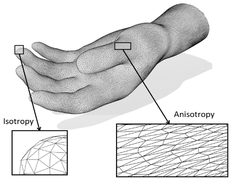
The computer graphics field represents shapes in the virtual world through triangle mesh. Traditionally, it is believed that isotropic triangles — where each side of the triangle has the same length regardless of direction — are the best representation of shapes.
However, the aggregate of these uniform triangles can create edges or bumps that are not on the original objects. Because triangle sides can differ in anisotrophic images, creating images with this technique would allow the user flexibility to more accurately represent object edges or folds.
Guo and his team found that replacing isotropic triangles with anisotropic triangles in the particle-based method of creating images resulted in smoother representations of objects. Depending on the curvature of the objects, the technique can generate the image up to 125 times faster than common approaches.
For example, 155 seconds to create a circular image with Guo’s approach, versus more than 19,500 seconds for a common approach to generate an image of similar quality.
Objects using anisotropic triangles are of a more accurate quality, and most noticeable to the human eye when it comes to wrinkles and movement of clothes on human representatives.
Modeling organs
[+]
Isotropy vs. anisotropy (credit: Zichun Zhong et al./SIGGRAPH)
The next step of this research is moving from representing the surface of 3D objects to representing 3D volume. “If we are going to create accurate representations of human organs, we need to account for the movement of cells below the organ’s surface,” Guo said.
Zichun Zhong, research assistant in computer science and PhD candidate at UT Dallas, was also involved in this research. Researchers from the University of Hong Kong, Inria Nancy Grand Est in France, Nvidia Corporation in California and UT Southwestern Medical Center also participated.
“These types of images are used in movies, video games, Computer-Aided Design (CAD), Computer-Aided Manufacturing (CAM), computational fluid dynamics (CFD) fields, scientific visualization, architecture design, etc.,” Zhong explained to KurzweilAI.
“It can work better to capture the behavior of physical phenomena, such as such as the flow of water or air across the Earth, the deformation and wrinkles of clothes on the human body, or in mechanical and other types of engineering designs. Medical scientists hope this technique will also lead to greater accuracy in models of human organs to more effectively treat human diseases, such as cancer.
“If we can find good commercial partners and attractive applications, it will appear on the market within several months.”

Abstract of SIGGRAPH 2013 presentation
This paper introduces a particle-based approach for anisotropic sur- face meshing. Given an input polygonal mesh endowed with a Rie- mannian metric and a specified number of vertices, the method generates a metric-adapted mesh. The main idea consists of mapping the anisotropic space into a higher dimensional isotropic one, called “embedding space”. The vertices of the mesh are generated by uniformly sampling the surface in this higher dimensional embedding space, and the sampling is further regularized by optimizing an energy function with a quasi-Newton algorithm. All the computations can be re-expressed in terms of the dot product in the embedding space, and the Jacobian matrices of the mappings that connect different spaces. This transform makes it unnecessary to explicitly represent the coordinates in the embedding space, and also provides all necessary expressions of energy and forces for efficient computations. Through energy optimization, it naturally leads to the desired anisotropic particle distributions in the original space. The triangles are then generated by computing the Restricted Anisotropic Voronoi Diagram and its dual Delaunay triangulation. We compare our results qualitatively and quantitatively with the state-of-the-art in anisotropic surface meshing on several examples, using the standard measurement criteria.


(¯`*• Global Source and/or more resources at http://goo.gl/zvSV7 │ www.Future-Observatory.blogspot.com and on LinkeIn Group's "Becoming Aware of the Futures" at http://goo.gl/8qKBbK │ @SciCzar │ Point of Contact: www.linkedin.com/in/AndresAgostini

Carnegie Mellon computer searches web 24/7 to analyze images and teach itself common sense

NEIL program labels images, learns associations with minimal help from people
November 22, 2013
(Credit: Carnegie Mellon University)
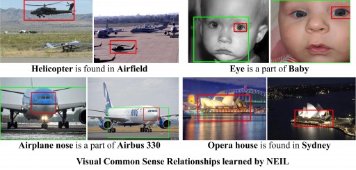
A computer program called the Never Ending Image Learner (NEIL) is now running 24 hours a day at Carnegie Mellon University, searching the Web for images, doing its best to understand them. And as it builds a growing visual database, it is gathering common sense on a massive scale.
NEIL leverages recent advances in computer vision that enable computer programs to identify and label objects in images, to characterize scenes and to recognize attributes, such as colors, lighting and materials, all with a minimum of human supervision. In turn, the data it generates will further enhance the ability of computers to understand the visual world.
But NEIL also makes associations between these things to obtain common sense information: cars often are found on roads, buildings tend to be vertical, and ducks look sort of like geese.
“Images are the best way to learn visual properties,” said Abhinav Gupta, assistant research professor in Carnegie Mellon’s Robotics Institute. “Images also include a lot of common sense information about the world. People learn this by themselves and, with NEIL, we hope that computers will do so as well.”
Since late July, the NEIL program has analyzed three million images, identifying 1,500 types of objects in half a million images and 1,200 types of scenes in hundreds of thousands of images. It has connected the dots to learn 2,500 associations from thousands of instances.
Drum (percussion) objects identified by NEIL (credit: CMU)
You can view NEIL’s findings at the project website (or help train it): http://www.neil-kb.com.
World’s largest structured visual knowledge base
One motivation for the NEIL project is to create the world’s largest visual structured knowledge base, where objects, scenes, actions, attributes and contextual relationships are labeled and catalogued.
“What we have learned in the last 5-10 years of computer vision research is that the more data you have, the better computer vision becomes,” Gupta said.
Some projects, such as ImageNet and Visipedia, have tried to compile this structured data with human assistance. But the scale of the Internet is so vast — Facebook alone holds more than 200 billion images — that the only hope to analyze it all is to teach computers to do it largely by themselves.
Shrivastava said NEIL can sometimes make erroneous assumptions that compound mistakes, so people need to be part of the process. A Google Image search, for instance, might convince NEIL that “pink” is just the name of a singer, rather than a color.
“People don’t always know how or what to teach computers,” he observed. “But humans are good at telling computers when they are wrong.”
People also tell NEIL what categories of objects, scenes, etc., to search and analyze. But sometimes, what NEIL finds can surprise even the researchers. Gupta and his team had no idea that a search for F-18 would identify not only images of a fighter jet, but also of F18-class catamarans.
As its search proceeds, NEIL develops subcategories of objects — cars come in a variety of brands and models. And it begins to notice associations — that zebras tend to be found in savannahs, for instance, and that stock trading floors are typically crowded.
NEIL is computationally intensive, the research team noted. The program runs on two clusters of computers that include 200 processing cores.
Practical uses
NEIL’s knowledge can be used wherever machine perception is required (e.g., image retrieval, robotics applications, object and scene recognition, describing images, visual properties of objects and even visual surveillance,” Gupta explained to KurzweilAI.
“NEIL has analyzed more than 5 million images and built a database of 0.5 million images and 3000 relationships in 4 months. The NEIL visual knowledge base also includes visual models of concepts (e.g., car, crowded, trading floor) and relationships between concepts (e.g., cars have wheels, trading floors are crowded). These models and relationships will be made available for academic research use. We also invite academic users to  submit concepts that they would like NEIL to learn  and later use these models for their own research.
“Once the technology is mature (hopefully in the near future), we expect NEIL’s knowledge base to have multiple commercial applications.”
The research is supported by the Office of Naval Research and Google Inc.

Abstract of International Conference on Computer vision (ICCV) paper
NEIL (Never Ending Image Learner) is a computer program that runs 24 hours per day and 7 days per week to automatically extract visual knowledge from Internet data. NEIL uses a semi-supervised learning algorithm that jointly discovers common sense relationships (e.g., “Corolla is a kind of/looks similar to Car”,“Wheel is a part of Car”) and labels instances of the given visual categories. It is an attempt to develop the world’s largest visual structured knowledge base with minimum human labeling effort. As of 10th October 2013, NEIL has been continuously running for 2.5 months on 200 core cluster (more than 350K CPU hours) and has an ontology of 1152 object categories, 1034 scene categories and 87 attributes. During this period, NEIL has discovered more than 1700 relationships and has labeled more than 400K visual instances.

(¯`*• Global Source and/or more resources at http://goo.gl/zvSV7 │ www.Future-Observatory.blogspot.com and on LinkeIn Group's "Becoming Aware of the Futures" at http://goo.gl/8qKBbK │ @SciCzar │ Point of Contact: www.linkedin.com/in/AndresAgostini
Thursday, November 21, 2013

Using a CT scan and 3D printer to recreate a fossil

November 21, 2013
3d_print_of_fossil
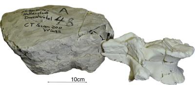
A 3D printed object (right) next to the original unprepared plaster jacket (credit: Courtesy of Radiology and RSNA)
Data from computed tomography (CT) scans can be used with 3D printers to make accurate copies of fossilized bones, according to new research published online in the journal Radiology.
Fossils are often stored in plaster casts, or jackets, to protect them from damage. Getting information about a fossil typically requires the removal of the plaster and all the sediment surrounding it, which can lead to loss of material or even destruction of the fossil itself.
German researchers used CT and 3-D printers to nondestructively separate fossilized bone from its surrounding sediment matrix and produce a 3D print of the fossilized bone itself.
“The most important benefit of this method is that it is non-destructive, and the risk of harming the fossil is minimal,” said study author Ahi Sema Issever, M.D., from the Department of Radiology at Charité Campus Mitte in Berlin. “Also, it is not as time-consuming as conventional preparation.”
Tracing an unidentified buried fossil
[+]jurassic_park
A future Jurassic Park movie sequel could call on 3D printers for more accurate models (credit: Universal Pictures)
Issever and colleagues applied the method to an unidentified fossil from the Museum für Naturkunde, a major natural history museum in Berlin.
The fossil and others like it were buried under rubble in the basement of the museum after a World War II bombing raid. Since then, museum staff members have had difficulty sorting and identifying some of the plaster jackets.
Researchers performed CT on the unidentified fossil with a 320-slice multi-detector system. The different attenuation, or absorption of radiation, through the bone compared with the surrounding matrix enabled clear depiction of a fossilized vertebral body.
After studying the CT scan and comparing it to old excavation drawings, the researchers were able to trace the fossil’s origin to the Halberstadt excavation, a major dig from 1910 to 1927 in a clay pit south of Halberstadt, Germany. In addition, the CT study provided valuable information about the condition and integrity of the fossil, showing multiple fractures and destruction of the front rim of the vertebral body.
Furthermore, the CT dataset helped the researchers build an accurate reconstruction of the fossil with selective laser sintering, a technology that uses a high-powered laser to fuse together materials to make a 3-D object.
Digital models of the objects can also be transferred rapidly among researchers, and endless numbers of exact copies may be produced and distributed, greatly advancing scientific exchange, Issever said. The technology could enables a global interchange of unique fossils with museums, schools, and other settings.

Abstract of Radiology paper
Purpose — To demonstrate the feasibility of using computed tomography (CT) to confirm the identity of an unprepared fossil and to use the CT dataset to separate the fossilized bone from its surrounding sediment matrix and produce a three-dimensional (3D) print.
Materials and Methods — The examined object was a plaster jacket containing an unprepared fossil. CT was performed with a 320-section multidetector unit. A marching cube-based method was used to transform the voxel CT dataset into triangle-based, editable geometry. Then, a comprehensive postprocessing step was performed to isolate the geometry of the vertebra from its surrounding fossilized matrix. Finally, the resulting polygon mesh describing only the vertebra was used for a physical 3D reconstruction by using a selective laser sintering machine.
Results — The CT examination provided enough data to assign the fossil to the genus Plateosaurus. In addition, much valuable information about the fossil has been gained—in particular the visualization of multiple fractures and the destruction of the anterior rim of the vertebral body. Finally, the results show that the 3D print generated, including the fractures and the anterior destruction, may be considered an accurate copy of the bone with the unprepared fossil.
Conclusion — The authors demonstrated the feasibility and potential utility of combining CT with 3D printing, providing a nondestructive method to future paleontologists.


(¯`*• Global Source and/or more resources at http://goo.gl/zvSV7 │ www.Future-Observatory.blogspot.com and on LinkeIn Group's "Becoming Aware of the Futures" at http://goo.gl/8qKBbK │ @SciCzar │ Point of Contact: www.linkedin.com/in/AndresAgostini

World’s smallest FM radio transmitter

Could lead to ultrathin, more-power-efficient cell phones
November 21, 2013
smallest_fm_transmitter
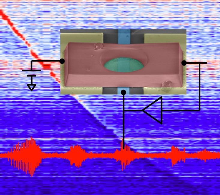
Placing a sheet of atomically thin graphene into a feedback circuit causes spontaneous self-oscillation that can be tuned to create frequency modulated (FM) signals (credit: Changyao Chen, Sunwoo Lee, Columbia University)
In another major new application of graphene, Columbia Engineering researchers have taken advantage of graphene’s special properties — its mechanical strength and electrical conductivity — to develop a nanomechanical system that can create FM signals — in effect, the world’s smallest FM radio transmitter.
“This is an important first step in advancing wireless signal processing and designing ultrathin, efficient cell phones, Mechanical Engineering Professor James Hone said. The miniaturized devices can also be put on the same chip that’s used for data processing, he added.
NEMS replacing MEMS
Graphene, a single atomic layer of carbon, is the strongest material known to man, and also has electrical properties superior to the silicon used to make the chips found in modern electronics.
The combination of these properties makes graphene an ideal material for nanoelectromechanical systems (NEMS), which are scaled-down versions of the microelectromechanical systems (MEMS) used widely for sensing of vibration and acceleration. For example, Hone explains, MEMS sensors figure out how your smartphone or tablet is tilted to rotate the screen.
In this new study, the team took advantage of graphene’s mechanical “stretchability” to tune the output frequency of their custom oscillator, creating a nanomechanical version of an electronic component known as a voltage controlled oscillator (VCO).
With a VCO, explains Hone, it is easy to generate a frequency-modulated (FM) signal, which is used for FM radio broadcasting. The team built a graphene NEMS whose frequency was about 100 megahertz, which lies right in the middle of the FM radio band (87.7 to 108 MHz).
They used low-frequency musical signals (both pure tones and songs from an iPhone) to modulate the 100 MHz carrier signal from the graphene, and then retrieved the musical signals again using an ordinary FM radio receiver.
“This device is by far the smallest system that can create such FM signals,” says Hone.
Wireless applications
[+]
A printed circuit board inside a Nokia 3210 cell phone, circa 1999. Most of these kinds of components have since been miniaturized; a future graphene NEMS system could further reduce the number of discrete components by moving their functions into a chip. (Credit: Martin Brož/Wikimedia Commons)
While graphene NEMS will not be used to replace conventional radio transmitters, they have many applications in wireless signal processing.
“Today’s cell phones have more computing power than systems that used to occupy entire rooms, explained Electrical Engineering Professor Kenneth Shepard.
“However, some types of devices, particularly those involved in creating and processing radio-frequency signals, are much harder to miniaturize.
“These “off-chip” components take up a lot of space and electrical power. In addition, most of these components cannot be easily tuned in frequency, requiring multiple copies to cover the range of frequencies used for wireless communication.”
Graphene NEMS can address both problems:  they are very compact and easily integrated with other types of electronics, and their frequency can be tuned over a wide range because of graphene’s tremendous mechanical strength.
“There is a long way to go toward actual applications in this area,” notes Hone, “but this work is an important first step. The Hone and Shepard groups are now working on improving the performance of the graphene oscillators to have lower noise. At the same time, they are also trying to demonstrate integration of graphene NEMS with silicon integrated circuits, making the oscillator design even more compact.
This work is supported by Qualcomm Innovation Fellowship 2012 and the U.S. Air Force, using facilities at the Cornell Nano-Scale Facility and the Center for Engineering and Physical Science Research (CEPSR) Clean Room at Columbia University.

Abstract of Nature Nanotechnology paper
Oscillators, which produce continuous periodic signals from direct current power, are central to modern communications systems, with versatile applications including timing references and frequency modulators. However, conventional oscillators typically consist of macroscopic mechanical resonators such as quartz crystals, which require excessive off-chip space. Here, we report oscillators built on micrometre-size, atomically thin graphene nanomechanical resonators, whose frequencies can be electrostatically tuned by as much as 14%. Self-sustaining mechanical motion is generated and transduced at room temperature in these oscillators using simple electrical circuitry. The prototype graphene voltage-controlled oscillators exhibit frequency stability and a modulation bandwidth sufficient for the modulation of radiofrequency carrier signals. As a demonstration, we use a graphene oscillator as the active element for frequency-modulated signal generation and achieve efficient audio signal transmission.

(¯`*• Global Source and/or more resources at http://goo.gl/zvSV7 │ www.Future-Observatory.blogspot.com and on LinkeIn Group's "Becoming Aware of the Futures" at http://goo.gl/8qKBbK │ @SciCzar │ Point of Contact: www.linkedin.com/in/AndresAgostini

Chaotic physics in ferroelectric materials may allow for brain-like computing

November 21, 2013
[+]
An illustration of memcomputing (credit: ORNL)
Unexpected behavior in ferroelectric materials explored by researchers at the Department of Energy’s Oak Ridge National Laboratory supports a new approach to information storage and processing called “memcomputing,” or memristor-based computing.
Ferroelectric materials are known for their ability to spontaneously switch polarization when an electric field is applied.
So using a scanning probe microscope, the ORNL-led team took advantage of this property to draw areas of switched polarization called domains on the surface of a ferroelectric material.
Unexpected chaotic patterns
To the researchers’ surprise, when written in dense arrays, the domains began forming complex and unpredictable patterns on the material’s surface.
“When we reduced the distance between domains, we started to see things that should have been completely impossible,” said ORNL’s Anton Ievlev, the first author on the paper published in Nature Physics.
[+]
A scanning probe microscope tip creating a domain with a ring of surface charge (credit: A. V. Ievlev et al/Nature Physics)
“All of a sudden, when we tried to draw a domain, it wouldn’t form, or it would form in an alternating pattern like a checkerboard.
At first glance, it didn’t make any sense. We thought that when a domain forms, it forms. It shouldn’t be dependent on surrounding domains.”
After studying patterns of domain formation under varying conditions, the researchers realized the complex behavior could be explained through chaos theory.
One domain would suppress the creation of a second domain nearby but facilitate the formation of one farther away — a precondition of chaotic behavior, says ORNL’s Sergei Kalinin, who led the study.
Brain-like computing

Collaborator Yuriy Pershin of the University of South Carolina explains that the team’s system possesses key characteristics needed for memcomputing, an emergent computing paradigm in which information storage and processing occur on the same physical platform.
“Memcomputing is basically how the human brain operates: Neurons and their connections–synapses — can store and process information in the same location,” Pershin said.
“Potentially, the observed domain intermittency in ferroelectric materials could be used to create a novel generation of information processing devices, which store and process information at the same physical location,” Pershin explained to KurzweilAI.
“Specifically, we are thinking about binary logic devices in which two possible directions of ferroelectric domain polarization could be naturally used to encode two logic states: 0 and 1. While the conventional technology requires several transistors to realize a logic gate, ferroelectric materials offer a transistor-less approach to logic, in certain sense similar to information processing and storage in actual brains.
“Additionally, the discovered domain interaction effect offers some interesting opportunities in research. In particular, it can be used as a tool to study intriguing physics of complex dynamical systems showing, for example a controllable transition to chaos. Using our system, one can perform, for instance, bench top emulation of different systems otherwise not available experimentally.
As for realization in commercial products, Pershin said multiple steps are needed. “In particular, in our setup, ferroelectric domains are switched by a moving STM tip. An actual chip, however, should be designed without any moving parts. We do not know exactly how hard-wired electrodes will influence the interaction among ferroelectric domains, for example.”
What makes this research unique
A study in Nature (464, 873-876, 8 April 2010) also demonstrates binary logic operations with memory resistive devices. But in the Oak Ridge Lab work, ferroelectric materials sandwiched between metal electrodes are essentially capacitive structures with potentially smaller energy dissipations compared to resistive devices.
Another related paper is arXiv:1306.6133, introducing a memcapacitive dynamic computing random access memory.
“These previous works demonstrate or suggest logic operations with physically distinct memristive or memcapacitive devices, while our discovery shows that one can use the same physical piece of material to store multiple bits of information and perform logic — an important advance,” said Pershin.

Abstract of Nature Physics paper
Memristive materials and devices, which enable information storage and processing on one and the same physical platform, offer an alternative to conventional von Neumann computation architectures. Their continuous spectra of states with intricate field-history dependence give rise to complex dynamics, the spatial aspect of which has not been studied in detail yet. Here, we demonstrate that ferroelectric domain switching induced by a scanning probe microscopy tip exhibits rich pattern dynamics, including intermittency, quasiperiodicity and chaos. These effects are due to the interplay between tip-induced polarization switching and screening charge dynamics, and can be mapped onto the logistic map. Our findings may have implications for ferroelectric storage, nanostructure fabrication and transistor-less logic.


(¯`*• Global Source and/or more resources at http://goo.gl/zvSV7 │ www.Future-Observatory.blogspot.com and on LinkeIn Group's "Becoming Aware of the Futures" at http://goo.gl/8qKBbK │ @SciCzar │ Point of Contact: www.linkedin.com/in/AndresAgostini