New hologram technology created by nanoantennas on a ‘metasurface’
A potentially revolutionary new technology for advanced sensors,
high-resolution displays, and information processing
November 19, 2013
[+]
Researchers have created tiny holograms using a “metasurface” capable
of the ultra-efficient control of light, representing a potential new
technology for advanced sensors, high-resolution displays and
information processing.
Researchers
have created tiny holograms using a “metasurface” capable of
ultra-efficient control of light, representing a potential new
technology for advanced sensors, high-resolution displays and
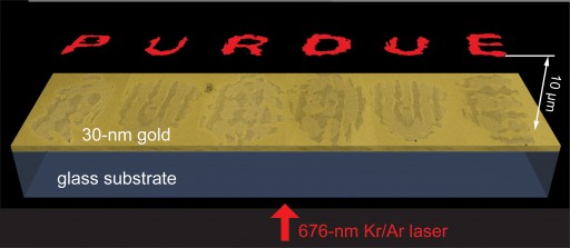
information processing. To demonstrate the technology, researchers
created a hologram of the word PURDUE smaller than 100 microns wide, or
roughly the width of a human hair. (Credit: Xingjie Ni/Birck
Nanotechnology Center)
The metasurface, thousands of V-shaped nanoantennas formed into an ultrathin gold foil, could make possible “planar photonics” devices and optical switches small enough to be integrated into computer chips for information processing, sensing and telecommunications, said Alexander Kildishev, associate research professor of electrical and computer engineering at Purdue University.
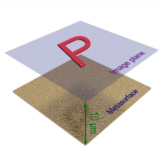
Laser light shines through the nanoantennas, creating the hologram 10 microns above the metasurface. To demonstrate the technology, researchers created a hologram of the word PURDUE smaller than 100 microns wide, or roughly the width of a human hair.
“If we can shape characters, we can shape different types of light beams for sensing or recording, or, for example, pixels for 3-D displays. Another potential application is the transmission and processing of data inside chips for information technology,” Kildishev said. “The smallest features — the strokes of the letters — displayed in our experiment are only 1 micron (millionth of a meter) wide. This is a quite remarkable spatial resolution.”
[+]
Metasurface 23 times thinner than the wavelength of visible light used
Laser
light shines through the metasurface from below, creating a hologram 10
microns above the structure (credit: Xingjie Ni/Birck Nanotechnology
Center)
Metasurfaces could make it possible to use single photons — the particles that make up light — for switching and routing in future computers.
While using photons would dramatically speed up computers and telecommunications, conventional photonic devices cannot be miniaturized because the wavelength of light is too large to fit in tiny components needed for integrated circuits.
Nanostructured metamaterials, however, are making it possible to reduce the wavelength of light, allowing the creation of new types of nanophotonic devices, said Vladimir M. Shalaev, scientific director of nanophotonics at Purdue’s Birck Nanotechnology Center and a distinguished professor of electrical and computer engineering.
“The most important thing is that we can do this with a very thin layer, only 30 nanometers, and this is unprecedented,” Shalaev said. “This means you can start to embed it in electronics, to marry it with electronics.”
The layer is about 1/23rd the width of the wavelength of light used to create the holograms. “To our knowledge, this is the thinnest hologram that can provide both amplitude and phase modulation in the visible wavelength range, [allowing for] generation of high-resolution, low-noise images,” the researchers said.
Under development for about 15 years, metamaterials owe their unusual potential to precision design on the scale of nanometers. Optical nanophotonic circuits might harness clouds of electrons called “surface plasmons” to manipulate and control the routing of light in devices too tiny for conventional lasers.
The researchers have shown how to control the intensity and phase, or timing, of laser light as it passes through the nanoantennas. Each antenna has its own “phase delay” — how much light is slowed as it passes through the structure. Controlling the intensity and phase is essential for creating working devices and can be achieved by altering the V-shaped antennas.
Findings are detailed in a research paper appearing on Friday (Nov. 15) in the journal Nature Communications.
The work is partially supported by U.S. Air Force Office of Scientific Research, Army research Office, and the National Science Foundation. Purdue has filed a provisional patent application on the concept.
Abstract of Nature Communications paper
Holography, a revolutionary 3-D imaging technique, has been developed for storing and recovering the amplitude and phase of light scattered by objects. Later, single-beam computer-generated phase holography was proposed for restoring the wavefront from a given incidence. However, because the phase modulation depends on the light propagation inside the material, the thickness of phase holograms usually remains comparable to the wavelength. Here we experimentally demonstrate ultra-thin metasurface holograms that operate in the visible range whose thickness is only 30 nm (approximately 1/23 of the operational wavelength). To our knowledge, this is the thinnest hologram that can provide both amplitude and phase modulation in the visible wavelength range, which generates high-resolution low-noise images. Using this technique, not only the phase, but potentially the amplitude of the incident wave can be efficiently controlled — expanding the route to new applications of ultra-thin and surface-confined photonic devices.
(¯`*• Global Source and/or more resources at http://goo.gl/zvSV7 │ www.Future-Observatory.blogspot.com and on LinkeIn Group's "Becoming Aware of the Futures" at http://goo.gl/8qKBbK │ @SciCzar │ Point of Contact: www.linkedin.com/in/AndresAgostini
 Washington