Seeing cells through silicon microfluidic devices
October 3, 2013
[+]
Scientists at MIT and the University of Texas at Arlington (UTA) have developed
a new type of microscopy that can image cells through a silicon wafer,
allowing them to precisely measure the size and mechanical behavior of
cells behind the wafer.
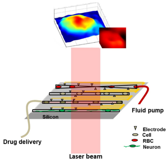
Schematic of the lab-on-chip system for the study of
mechanical, chemical, and electric perturbation of different types of cells
on silicon-based microfluidic and multi-electrode array platform.
Quantitative phase image (through silicon) of a human embryonic kidney cell and red blood cell is shown on the top. (Credit: B. Joshi et al./Scientific Reports)
The new technology, which relies on near-infrared light, could help scientists learn more about diseased or infected cells as they flow through silicon microfluidic devices.
“This has the potential to merge research in cellular visualization with all the exciting things you can do on a silicon wafer,” says Ishan Barman, a former postdoc in MIT’s Laser Biomedical Research Center (LBRC) and one of the lead authors of a paper describing the technology in the Oct. 2 issue of the journal Scientific Reports (open access).
The senior author is Samarendra Mohanty, an assistant professor of physics at UTA.
Silicon is commonly used to build “lab-on-a-chip” microfluidic devices, which can sort and analyze cells based on their molecular properties. Such devices have many potential applications in research and diagnostics, but they could be even more useful if scientists could image the cells inside the devices, says Barman, who is now an assistant professor of mechanical engineering at Johns Hopkins University.
To achieve that, Barman and colleagues took advantage of the fact that silicon is transparent to infrared and near-infrared wavelengths of light. They adapted a microscopy technique known as quantitative phase imaging, which works by sending a laser beam through a sample, then splitting the beam into two. By recombining those two beams and comparing the information carried by each one, the researchers can determine the sample’s height and its refractive index — a measure of how much the material forces light to bend as it passes through.
Traditional quantitative phase imaging uses a helium neon laser, which produces visible light, but for the new system the researchers used a titanium sapphire laser that can be tuned to infrared and near-infrared wavelengths (they found that light with a wavelength of 980 nanometers worked best).
Using this system, the researchers measured changes in the height of red blood cells, with nanoscale sensitivity, through a silicon wafer similar to those used in most electronics labs.
Examples of uses:
- As red blood cells flow through the body, they often have to squeeze through very narrow vessels. When these cells are infected with malaria, they lose this ability to deform, and form clogs in tiny vessels. The new microscopy technique could help scientists study how this happens, the researchers say. It could also be used to study the dynamics of the malformed blood cells that cause sickle cell anemia.
- The researchers also used their new system to monitor human embryonic kidney cells as pure water was added to their environment — a shock that forces the cells to absorb water and swell up. The researchers were able to measure how much the cells distended and calculate the change in their index of refraction.
- Mohanty’s lab at UTA is now using the system to study how neurons grown on a silicon wafer communicate with each other.
“This is an exciting new direction that is likely to open up enormous opportunities for quantitative phase imaging,” says Gabriel Popescu, an assistant professor of electrical engineering and computer science at the University of Illinois at Urbana-Champaign who was not part of the research team. “The possibilities are endless: From micro- and nanofluidic devices to structured substrates, the devices could target applications ranging from molecular sensing to whole-cell characterization and drug screening in cell populations,” he says.
In the Scientific Reports paper, the researchers used silicon wafers that were about 150 to 200 microns thick, but they have since shown that thicker silicon can be used if the wavelength of light is increased into the infrared range. The researchers are also working on modifying the system so that it can image in three dimensions, similar to a CT scan.
Other lead authors of the paper are former MIT postdoc Narahara Chari Dingari and UTA graduate students Bipin Joshi and Nelson Cardenas. Other authors are former MIT postdoc Jaqueline Soares, currently an assistant professor at Federal University of Ouro Preto, Brazil, and Ramachandra Rao Dasari, associate director of the LBRC.
The research was funded by the National Institute of Biomedical Imaging and Bioengineering and Nanoscope Technologies, LLC.
Department of Chemistry
“MIT shows how blood cells change shape”
Abstract for Scientific Reports paper
We report a novel technique for label-free, rapid visualization of structure and dynamics of live cells with nanoscale sensitivity through traditionally opaque media. Specifically, by combining principles of near-infrared (NIR) spectroscopy and quantitative phase imaging, functional characterization of cellular structure and dynamics through silicon substrates is realized in our study. We demonstrate the efficacy of the new approach by full-field imaging of erythrocyte morphology in their native states with a nm path length sensitivity. Additionally, we observe dynamic variations of human embryonic kidney cells, through a silicon substrate, in response to hypotonic stimulation with ms temporal resolution that also provides unique insight into the underlying biophysical changes. The proposed technology is fundamentally suited for high-performance investigations of biological specimens and significantly expands the options for visualization in complex microfluidic devices fabricated on silicon.
(¯`*• Global Source and/or more resources at http://goo.gl/zvSV7 │ www.Future-Observatory.blogspot.com and on LinkeIn Group's "Becoming Aware of the Futures" at http://goo.gl/8qKBbK │ @SciCzar │ Point of Contact: www.linkedin.com/in/AndresAgostini
 Washington