Controlled atomic-layer crystal growth is ‘breakthrough’ for solar-cell efficiency
October 30, 2013

The
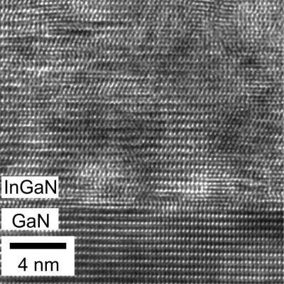
atomic arrangement of an InGaN/GaN interface created by layer-by-layer
atomic crystal growth. The new technique may lead to new developments in
solar-cell efficiency. (Credit: Arizona State University)
Researchers previously found that the atomic separation of the crystal layers of the InGaN alloy varies, which can lead to high levels of strain, breakdowns in growth, and fluctuations in the alloy’s chemical composition.
“Being able to ease the strain and increase the uniformity in the composition of InGaN is very desirable, but difficult to achieve,” said Arizona State University physics professor Fernando Ponce.
“Growth of these layers is similar to trying to smoothly fit together two honeycombs with different cell sizes, where size difference disrupts a periodic arrangement of the cells.”
Controlled crystal-layer growth
So the researchers developed a “metal-modulated epitaxy” approach that allows controlled atomic layer-by-layer growth of the material. Thin films grown with the epitaxy technique had almost ideal characteristics; the unexpected results came from strain relaxation at the first atomic layer of crystal growth.
The final crystal is more uniform and the lattice structures match up, resulting in a film that resembles a perfect crystal. “The luminosity was also like that of a perfect crystal. Something that no one in our field thought was possible.”
Eliminating these two defects (non-uniform composition and mismatched lattice alignment) ultimately means that solar photovoltaic devices (and LEDs) can now be developed that have much higher, more efficient performance, according to the researchers.
The InGaN alloy also forms the light emitting region of LEDs for illumination in the visible range and of laser diodes (LDs) in the blue-UV range.
Abstract of Applied Physics Letters paper
We have studied the properties of thick In x Ga1− x N films, with indium content ranging from x ∼ 0.22 to 0.67, grown by metal-modulated epitaxy. While the low indium-content films exhibit high density of stacking faults and dislocations, a significant improvement in the crystalline quality and optical properties has been observed starting at x ∼ 0.6. Surprisingly, the In x Ga1− x N film with x ∼ 0.67 exhibits high luminescence intensity, low defect density, and uniform full lattice-mismatch strain relaxation. The efficient strain relaxation is shown to be due to a critical thickness close to the monolayer range. These films were grown at low temperatures (∼400 °C) to facilitate indium incorporation and with precursor modulation to enhance surface morphology and metal adlayer diffusion. These findings should contribute to the development of growth techniques for nitride semiconductors under high lattice misfit conditions.
(¯`*• Global Source and/or more resources at http://goo.gl/zvSV7 │ www.Future-Observatory.blogspot.com and on LinkeIn Group's "Becoming Aware of the Futures" at http://goo.gl/8qKBbK │ @SciCzar │ Point of Contact: www.linkedin.com/in/AndresAgostini
 Washington