A bio-inspired method to attach graphene to silicon wafers for electronic devices
December 16, 2013
Graphene has outstanding electronic, optical and mechanical properties, but there has been no practical way to grow and transfer graphene for use in semiconductors with minimal defects — only discontinuous, nanometer-sized islands. The new process now opens up practical wafer-scale uses of graphene in electronics and photonics, for devices such as transistors, transparent conductive touch-screen panels, on-chip biosensors, and optoelectronic modulators.
Face-to-face transfer
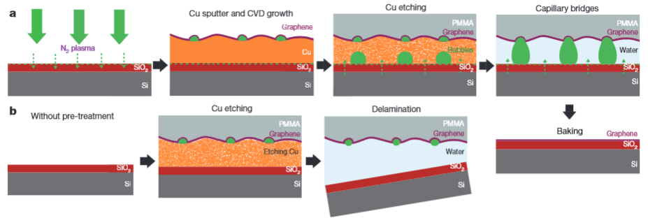
The researchers’ new process grows graphene on a copper catalyst layer, coating a silicon substrate. The copper is etched away while the graphene is held in place by bubbles that form capillary bridges, similar to those seen around the feet of beetles and tree frogs, keeping the feet firmly attached to submerged leaves via
[+]

llustration
of face-to-face method for transferring graphene mediated by capillary
bridges. (a) “Bubble seeding” by plasma treatment, chemical vapor
deposition growth, copper film etching (with a coating of Poly(methyl
methacrylate) for protection), formation of capillary bridges, and
removal of water (b) In the absence of plasma treatment, delamination of
the film results. (Credit: Libo Gao et al./Nature)
[+]
These bridges help keep the graphene attached to the silicon surface and prevent its delamination (separation of layers, creating cracks or folds) during the etching of the copper catalyst.
Frog attached to leaf (credit: Wikimedia Commons)
To facilitate the formation of capillary bridges, in a pre-treatment step, they inject gases into the wafer and a surfactant help to iron out any folds and creases created during the transfer process.
This novel process for growing graphene directly on silicon wafers and other stiff substrates will be very useful for the development of rapidly emerging graphene-on-silicon platforms, which have shown a promising range of applications, the researchers say.
Importantly, the “face-to-face transfer” method works with batch-processed semiconductor production lines, such as the fabrication of large-scale integrated circuits on silicon wafers.
The researchers plan to optimize the process to achieve high-throughput production of large-diameter (wafer-scale) graphene on silicon in a semiconductor production line. Talks are now underway with potential industry partners.
Abstract of Nature paper
Graphene has attracted worldwide interest since its experimental discovery, but the preparation of large-area, continuous graphene film on SiO2/Si wafers, free from growth-related morphological defects or transfer-induced cracks and folds, remains a formidable challenge. Growth of graphene by chemical vapour deposition on Cu foils has emerged as a powerful technique owing to its compatibility with industrial-scale roll-to-roll technology. However, the polycrystalline nature and microscopic roughness of Cu foils means that such roll-to-roll transferred films are not devoid of cracks and folds. High-fidelity transfer or direct growth of high-quality graphene films on arbitrary substrates is needed to enable wide-ranging applications in photonics or electronics, which include devices such as optoelectronic modulators, transistors, on-chip biosensors and tunnelling barriers. The direct growth of graphene film on an insulating substrate, such as a SiO2/Si wafer, would be useful for this purpose, but current research efforts remain grounded at the proof-of-concept stage, where only discontinuous, nanometre-sized islands can be obtained. Here we develop a face-to-face transfer method for wafer-scale graphene films that is so far the only known way to accomplish both the growth and transfer steps on one wafer. This spontaneous transfer method relies on nascent gas bubbles and capillary bridges between the graphene film and the underlying substrate during etching of the metal catalyst, which is analogous to the method used by tree frogs to remain attached to submerged leaves. In contrast to the previous wet or dry transfer results, the face-to-face transfer does not have to be done by hand and is compatible with any size and shape of substrate; this approach also enjoys the benefit of a much reduced density of transfer defects compared with the conventional transfer method. Most importantly, the direct growth and spontaneous attachment of graphene on the underlying substrate is amenable to batch processing in a semiconductor production line, and thus will speed up the technological application of graphene.
(¯`*• Global Source and/or more resources at http://goo.gl/zvSV7 │ www.Future-Observatory.blogspot.com and on LinkeIn Group's "Becoming Aware of the Futures" at http://goo.gl/8qKBbK │ @SciCzar │ Point of Contact: www.linkedin.com/in/AndresAgostini
 Washington