Densest array of carbon nanotubes grown to date
New technique could one day help improve the performance of microelectronics devices
September 27, 2013

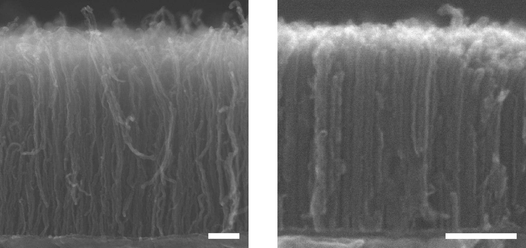
Scanning electron microscope images of CNT forests with low (left) and high density (right) (credit: AIP)
Such high-density nanotubes might one day replace some metal electronic components, such as interconnects, leading to faster devices.
Carbon nanotubes’ outstanding mechanical, electrical and thermal properties make them an alluring material to electronics manufacturers. However, until recently scientists believed that growing the high density of nanotubes needed for many microelectronics applications would be difficult.
“The high-density aspect is often overlooked in many carbon nanotube growth processes, and is an unusual feature of our approach,” says John Robertson, a professor in the electronic devices and materials group in the department of engineering at Cambridge. High-density forests are necessary for certain applications of carbon nanotubes, like electronic interconnects and thermal interface materials, he says.
Robertson and his colleagues grew carbon nanotubes on a conductive copper surface that was coated with co-catalysts cobalt and molybdenum. In a novel approach, the researchers grew them at lower temperature than is typical. Analysis of the interaction of metals by X-ray photoelectron spectroscopy revealed the creation of a more supportive substrate for the forests to root in. The subsequent nanotube growth exhibited the highest mass density reported so far.
“In microelectronics, this approach to growing high-density carbon nanotube forests on conductors can potentially replace and outperform the current copper-based interconnects in a future generation of devices,” says Cambridge researcher Hisashi Sugime.
In the future, more robust carbon nanotube forests may also help improve thermal interface materials, battery electrodes, and supercapacitors, he added.
While the new technique is intended for interconnects rather than semiconductors, it is conceivable it could be incorporated into potential future computer designs that use the carbon-nanotube field-effect transistor (CNFET) technology announced by Stanford University.
* Abstract of Appl. Phys. Lett. paper
We grow ultra-high mass density carbon nanotube forests at 450 °C on Ti-coated Cu supports using Co-Mo co-catalyst. X-ray photoelectron spectroscopy shows Mo strongly interacts with Ti and Co, suppressing both aggregation and lifting off of Co particles and, thus, promoting the root growth mechanism. The forests average a height of 0.38 μm and a mass density of 1.6 g cm−3. This mass density is the highest reported so far, even at higher temperatures or on insulators. The forests and Cu supports show ohmic conductivity (lowest resistance ∼22 kΩ), suggesting Co-Mo is useful for applications requiring forest growth on conductors.
(¯`*• Global Source and/or more resources at http://goo.gl/zvSV7 │ www.Future-Observatory.blogspot.com and on LinkeIn Group's "Becoming Aware of the Futures" at http://goo.gl/8qKBbK │ @SciCzar │ Point of Contact: www.linkedin.com/in/AndresAgostini
 Washington